SLAU917B October   2023  – February 2024 AFE20408


  1.   1
  2.   Description
  3.   Get Started
  4.   Features
  5.   Applications
  6.   6
  7. 1Evaluation Module Overview
    1. 1.1 Introduction
    2. 1.2 Kit Contents
    3. 1.3 Specification
    4. 1.4 Device Information
  8. 2Hardware
    1. 2.1 Hardware Setup
      1. 2.1.1 Hardware Theory of Operation
      2. 2.1.2 Jumper Definitions
      3. 2.1.3 Connector Definitions
      4. 2.1.4 Test Points
    2. 2.2 Hardware Overview
      1. 2.2.1 Electrostatic Discharge Caution
      2. 2.2.2 Connecting the FTDI Digital Controller
      3. 2.2.3 SPI Configuration
      4. 2.2.4 I2C Configuration
      5. 2.2.5 PAON Open Drain Circuit
  9. 3Software
    1. 3.1 Software Setup
      1. 3.1.1 Software Installation
    2. 3.2 Software Overview
      1. 3.2.1 Launching the Software
      2. 3.2.2 Software Features
        1. 3.2.2.1 Low Level Configuration Page
        2. 3.2.2.2 High Level Configuration Page
  10. 4Hardware Design Files
    1. 4.1 Schematics
    2. 4.2 PCB Layout
    3. 4.3 Bill of Materials
  11. 5Additional Information
    1.     Trademarks
  12. 6Revision History

PCB Layout

Figure 5-4 through Figure 5-7 show the board layout for the AFE20408EVM.
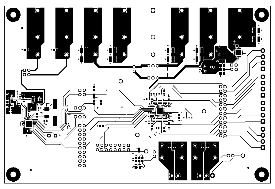
GUID-20231109-SS0I-BFRF-7WDZ-XMQPCX0FPNRV-low.pngFigure 4-4 AFE20408EVM PCB Top Layer Layout
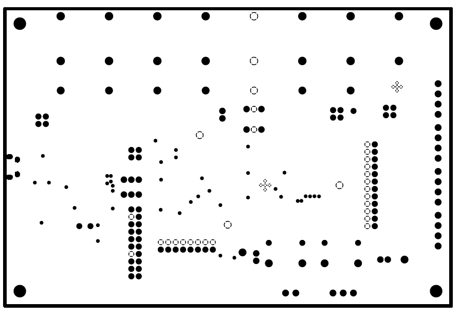
GUID-20231109-SS0I-GQC8-NCCN-W2P0FWCGRM63-low.pngFigure 4-5 AFE20408EVM PCB Mid Layer 1 Layout (Ground Plane)
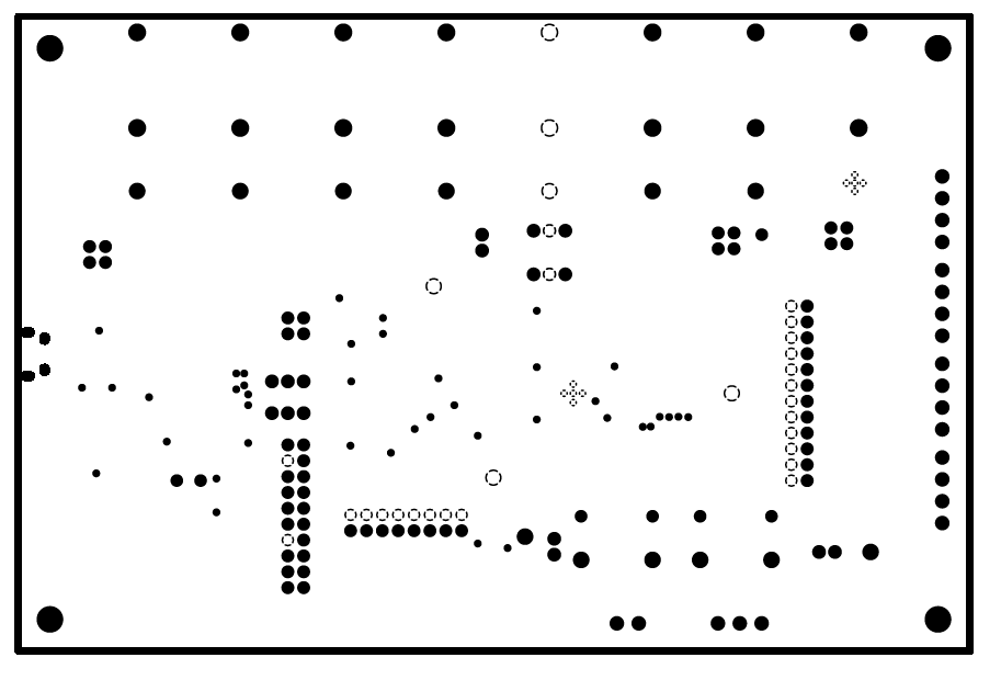
GUID-20231109-SS0I-DHV6-WHMD-QGMNMBPKKWNC-low.pngFigure 4-6 AFE20408EVM PCB Mid Layer 2 Layout (Ground Plane)
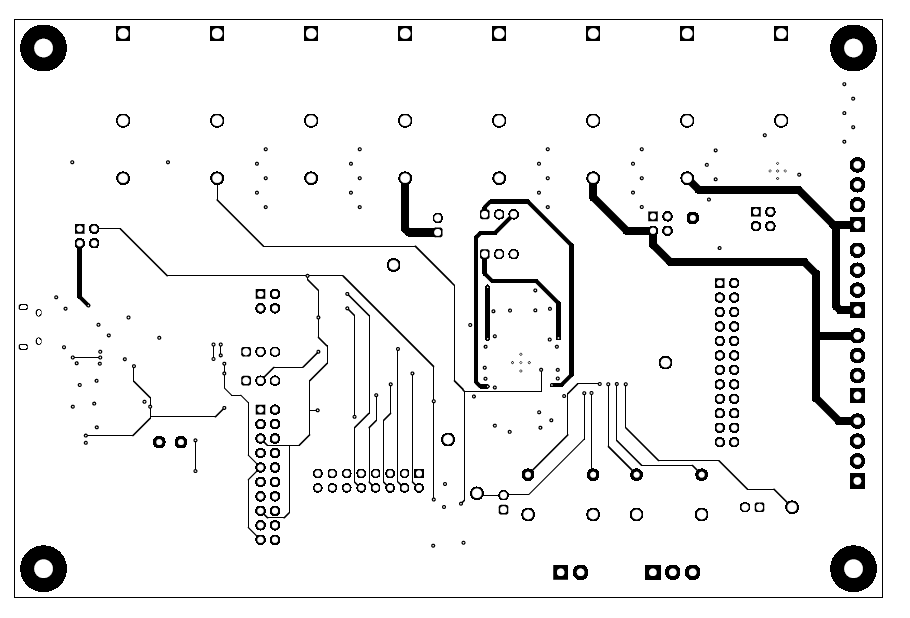
GUID-20231109-SS0I-XKDS-DDFW-XRFMVN7NT7KK-low.pngFigure 4-7 AFE20408EVM PCB Bottom Layer Layout