SLAU917B October   2023  – February 2024 AFE20408


  1.   1
  2.   Description
  3.   Get Started
  4.   Features
  5.   Applications
  6.   6
  7. 1Evaluation Module Overview
    1. 1.1 Introduction
    2. 1.2 Kit Contents
    3. 1.3 Specification
    4. 1.4 Device Information
  8. 2Hardware
    1. 2.1 Hardware Setup
      1. 2.1.1 Hardware Theory of Operation
      2. 2.1.2 Jumper Definitions
      3. 2.1.3 Connector Definitions
      4. 2.1.4 Test Points
    2. 2.2 Hardware Overview
      1. 2.2.1 Electrostatic Discharge Caution
      2. 2.2.2 Connecting the FTDI Digital Controller
      3. 2.2.3 SPI Configuration
      4. 2.2.4 I2C Configuration
      5. 2.2.5 PAON Open Drain Circuit
  9. 3Software
    1. 3.1 Software Setup
      1. 3.1.1 Software Installation
    2. 3.2 Software Overview
      1. 3.2.1 Launching the Software
      2. 3.2.2 Software Features
        1. 3.2.2.1 Low Level Configuration Page
        2. 3.2.2.2 High Level Configuration Page
  10. 4Hardware Design Files
    1. 4.1 Schematics
    2. 4.2 PCB Layout
    3. 4.3 Bill of Materials
  11. 5Additional Information
    1.     Trademarks
  12. 6Revision History

I2C Configuration

Figure 3-3 shows the AFE20408EVM configured for I2C communication.
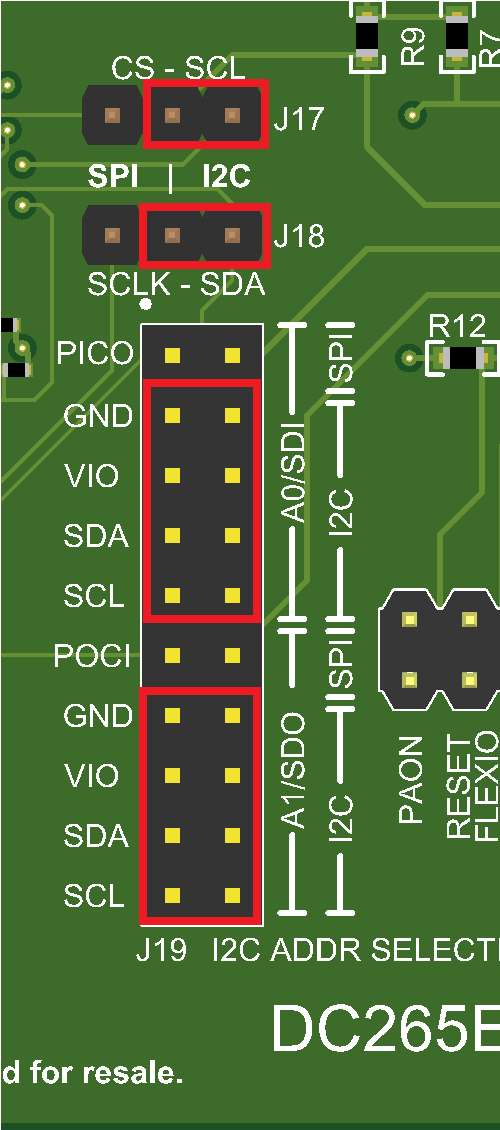
GUID-20231002-SS0I-QJ8W-MXJK-PG4P4F4RNX7V-low.pngFigure 2-3 AFE20408EVM Configuration I2C

The jumper connections on J19 determine the device address of the AFE20408. The following table shows the required configuration of the A1 and A0 jumpers for specific device addresses.

Table 2-7 I2C Device Address Map
A1

A0

[A6:A0]

GNDGND101 0000
GNDVIO101 0001
GNDSDA101 0010
GNDSCL101 0011
VIOGND101 0100
VIOVIO101 0101
VIOSDA101 0110
VIOSCL101 0111
SDAGND101 1000
SDAVIO101 1001
SDASDA101 1010
SDASCL101 1011
SCLGND101 1100
SCLVIO101 1101
SCLSDA101 1110
SCLSCL101 1111