SLAU919A November   2023  – June 2024


  1.   1
  2.   Description
  3.   Get Started
  4.   Features
  5.   Applications
  6.   6
  7. 1Evaluation Module Overview
    1. 1.1 Introduction
    2. 1.2 Kit Contents
    3. 1.3 Specification
    4. 1.4 Device Information
  8. 2Hardware
    1. 2.1 Hardware Setup
      1. 2.1.1 Hardware Theory of Operation
      2. 2.1.2 Jumper Definitions
      3. 2.1.3 Connector Definitions
      4. 2.1.4 Test Points
    2. 2.2 Hardware Overview
      1. 2.2.1 Electrostatic Discharge Caution
      2. 2.2.2 Connecting the FTDI Digital Controller
      3. 2.2.3 SPI Configuration
      4. 2.2.4 I2C Configuration
  9. 3Software
    1. 3.1 Software Setup
      1. 3.1.1 Software Installation
    2. 3.2 Software Overview
      1. 3.2.1 Launching the Software
      2. 3.2.2 Software Features
        1. 3.2.2.1 Low Level Configuration Page
        2. 3.2.2.2 High Level Configuration Page
  10. 4Hardware Design Files
    1. 4.1 Schematics
    2. 4.2 PCB Layout
    3. 4.3 Bill of Materials
  11. 5Additional Information
    1. 5.1 Trademarks
  12. 6Related Documentation
  13. 7Revision History

I2C Configuration

Figure 3-3 shows the DAC80502-01EVM configured for I2C communication.
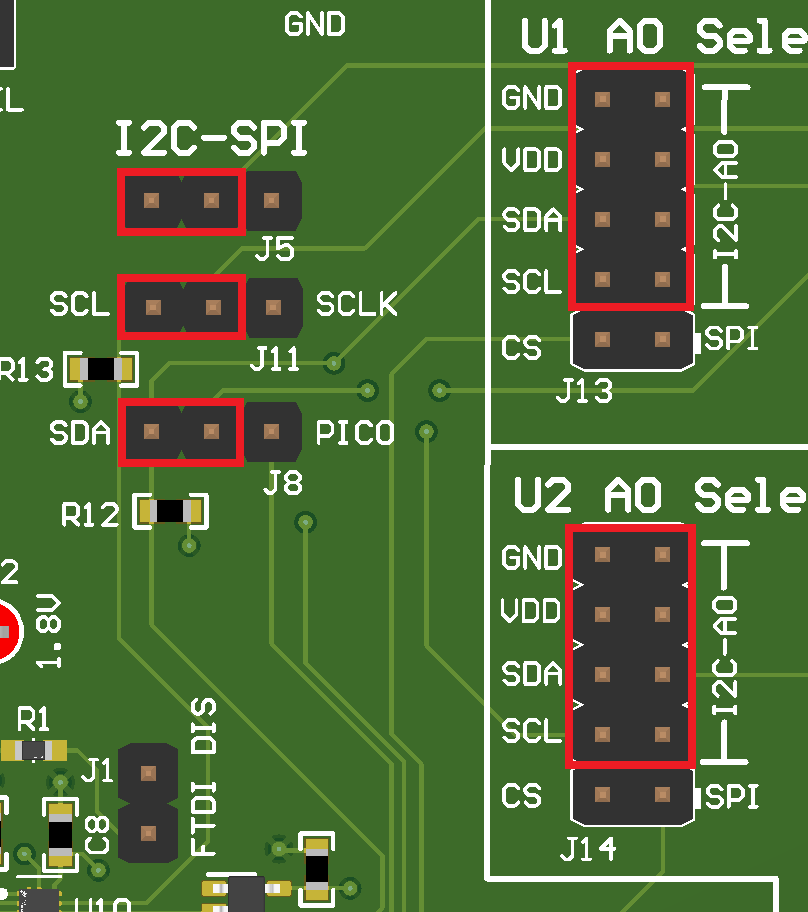
DAC80502-01EVM DAC80502-01EVM I2C Configuration Figure 2-4 DAC80502-01EVM I2C Configuration

The jumper connections on J13 and J14 determine the device address of the DAC80501 and DAC80502, respectively. Table 3-7 shows the required configuration of the two A0 jumpers for specific device addresses.

Table 2-7 I2C Device Address Map

A0 Connection

[A6:A0]

GND

1001 000

VDD

1001 001

SDA

1001 010

SCL

1001 011