SLAU947 October   2024 MSPM0G3519


  1.   1
  2.   Description
  3.   Get Started
  4.   Features
  5.   Applications
  6.   6
  7. 1Evaluation Module Overview
    1. 1.1 Introduction
    2. 1.2 Kit Contents
    3. 1.3 Specification
    4. 1.4 Device Information
  8. 2Hardware
    1. 2.1 Hardware Overview
    2. 2.2 Power Requirements
    3. 2.3 XDS110 Debug Probe
    4. 2.4 Measure Current Draw of the MSPM0G3519
    5. 2.5 Clocking
    6. 2.6 BoosterPack Plug-in Module Pinout
  9. 3Software
    1. 3.1 Software Development Options
    2. 3.2 Out-of-Box GUI
    3. 3.3 CCS Cloud
  10. 4Hardware Design Files
    1. 4.1 Schematics
    2. 4.2 PCB Layouts
    3. 4.3 Bill of Materials (BOM)
  11. 5Compliance Information
    1. 5.1 Compliance and Certifications
  12. 6Additional Information
    1. 6.1 Trademarks
  13. 7Related Documentation
    1. 7.1 Supplemental Content

PCB Layouts

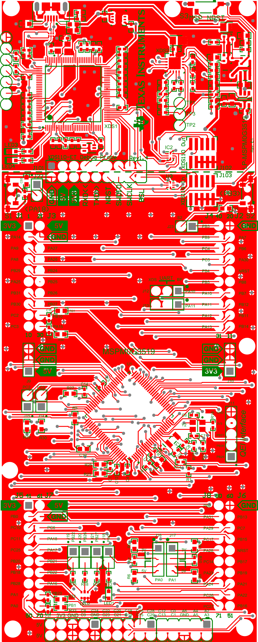
LP-MSPM0G3519 Top Layer and Overlay (1st
                        Layer)Figure 4-8 Top Layer and Overlay (1st Layer)
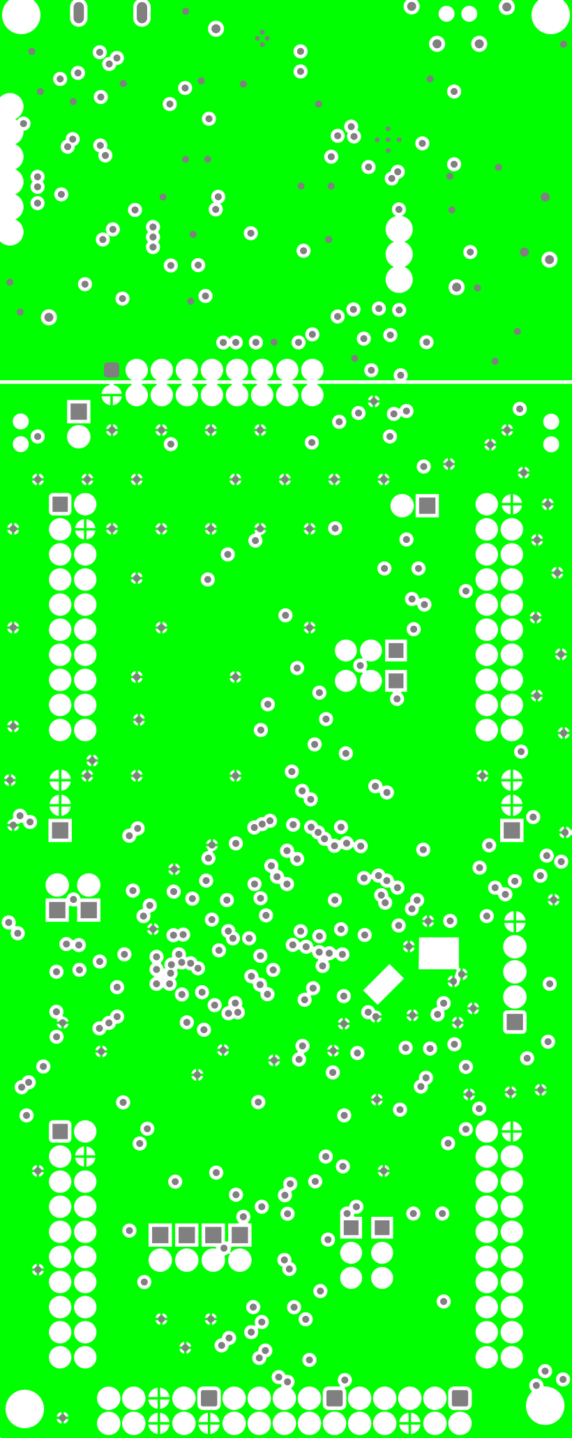
LP-MSPM0G3519 Ground Plane (3rd
                        Layer)Figure 4-10 Ground Plane (3rd Layer)
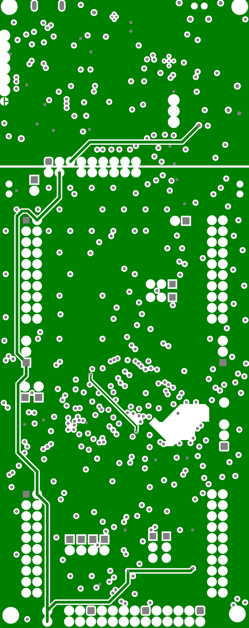
LP-MSPM0G3519 VCC Plane (2nd
                        Layer)Figure 4-9 VCC Plane (2nd Layer)
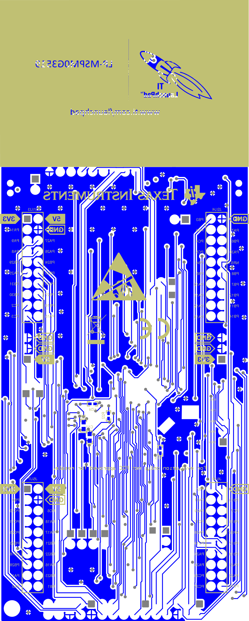
LP-MSPM0G3519 Bottom Layer and Overlay
                        (4th Layer)Figure 4-11 Bottom Layer and Overlay (4th Layer)