SLAU947 October   2024 MSPM0G3519


  1.   1
  2.   Description
  3.   Get Started
  4.   Features
  5.   Applications
  6.   6
  7. 1Evaluation Module Overview
    1. 1.1 Introduction
    2. 1.2 Kit Contents
    3. 1.3 Specification
    4. 1.4 Device Information
  8. 2Hardware
    1. 2.1 Hardware Overview
    2. 2.2 Power Requirements
    3. 2.3 XDS110 Debug Probe
    4. 2.4 Measure Current Draw of the MSPM0G3519
    5. 2.5 Clocking
    6. 2.6 BoosterPack Plug-in Module Pinout
  9. 3Software
    1. 3.1 Software Development Options
    2. 3.2 Out-of-Box GUI
    3. 3.3 CCS Cloud
  10. 4Hardware Design Files
    1. 4.1 Schematics
    2. 4.2 PCB Layouts
    3. 4.3 Bill of Materials (BOM)
  11. 5Compliance Information
    1. 5.1 Compliance and Certifications
  12. 6Additional Information
    1. 6.1 Trademarks
  13. 7Related Documentation
    1. 7.1 Supplemental Content

Schematics

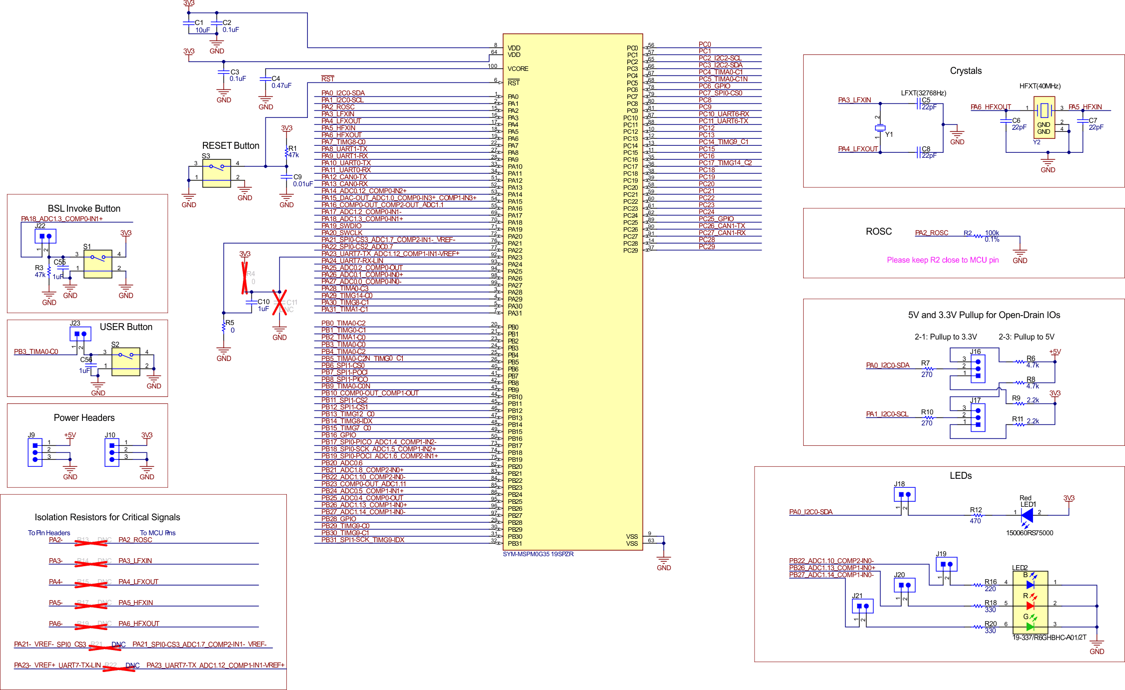
LP-MSPM0G3519 MSPM0G3519 Target Device
                    Schematic Figure 4-1 MSPM0G3519 Target Device Schematic
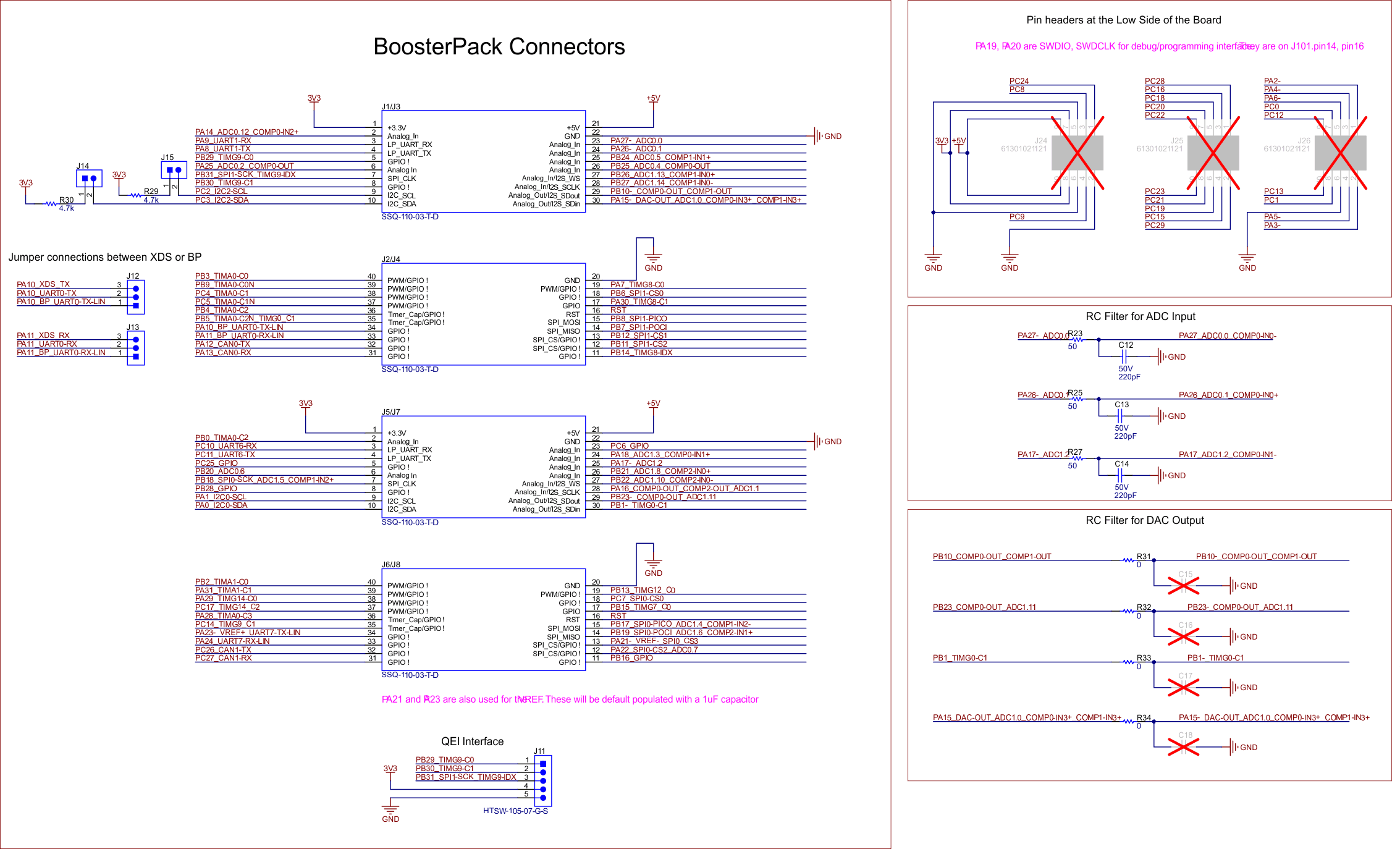
LP-MSPM0G3519 BoosterPack Connectors Figure 4-2 BoosterPack Connectors
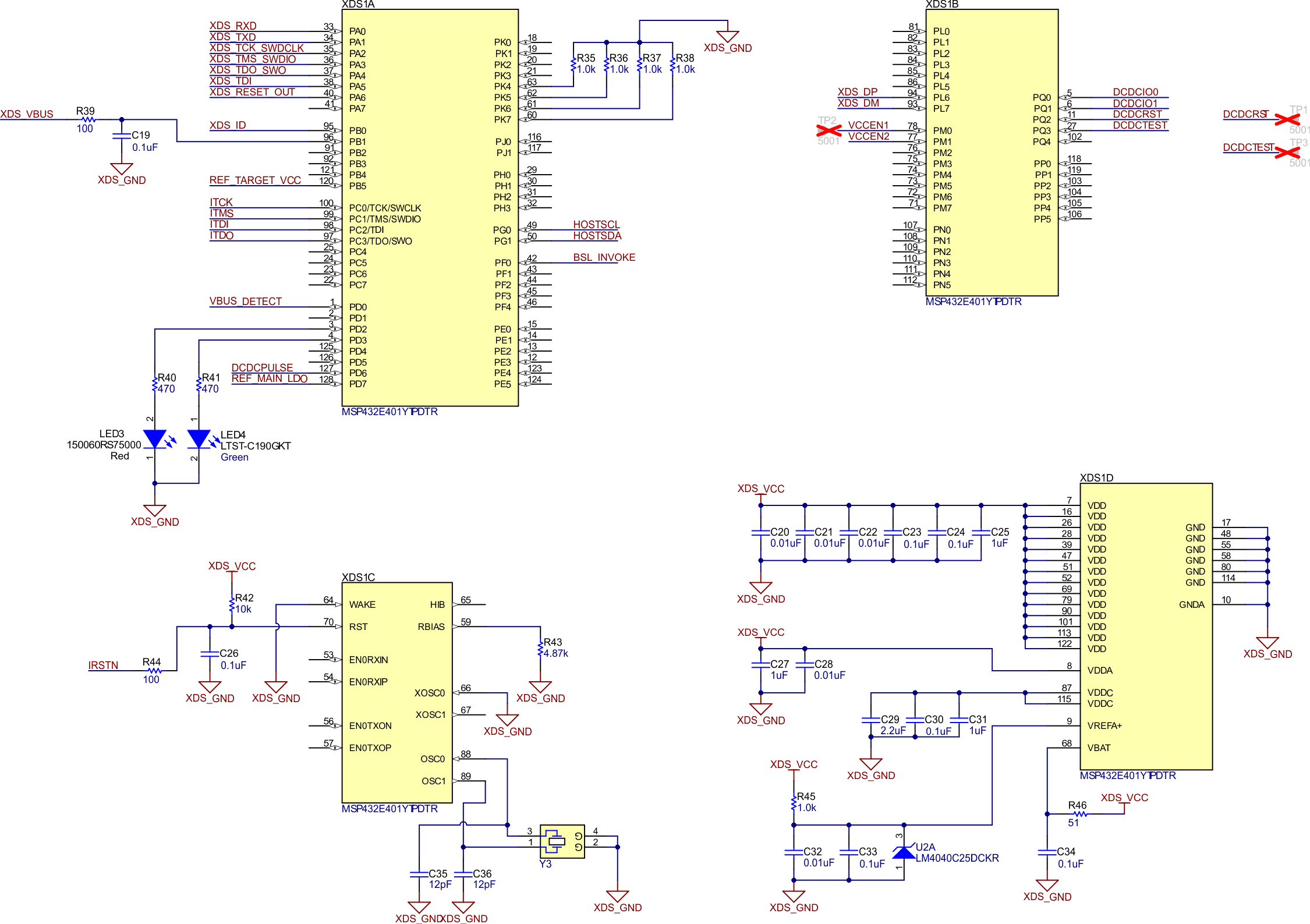
LP-MSPM0G3519 XDS110 Debug Probe Emulator
                    Schematic Figure 4-3 XDS110 Debug Probe Emulator Schematic
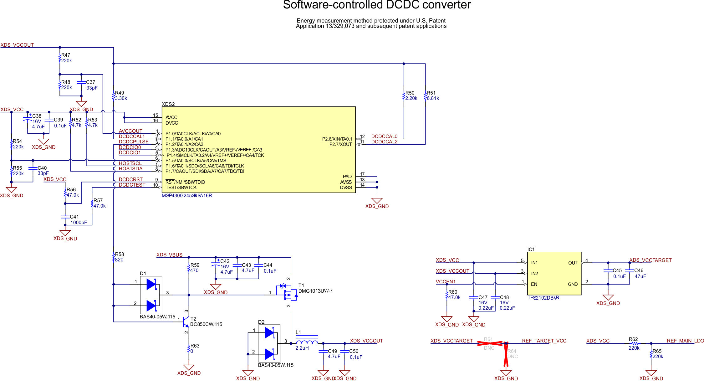
LP-MSPM0G3519 XDS110 EnergyTrace
                    Schematic Figure 4-4 XDS110 EnergyTrace Schematic
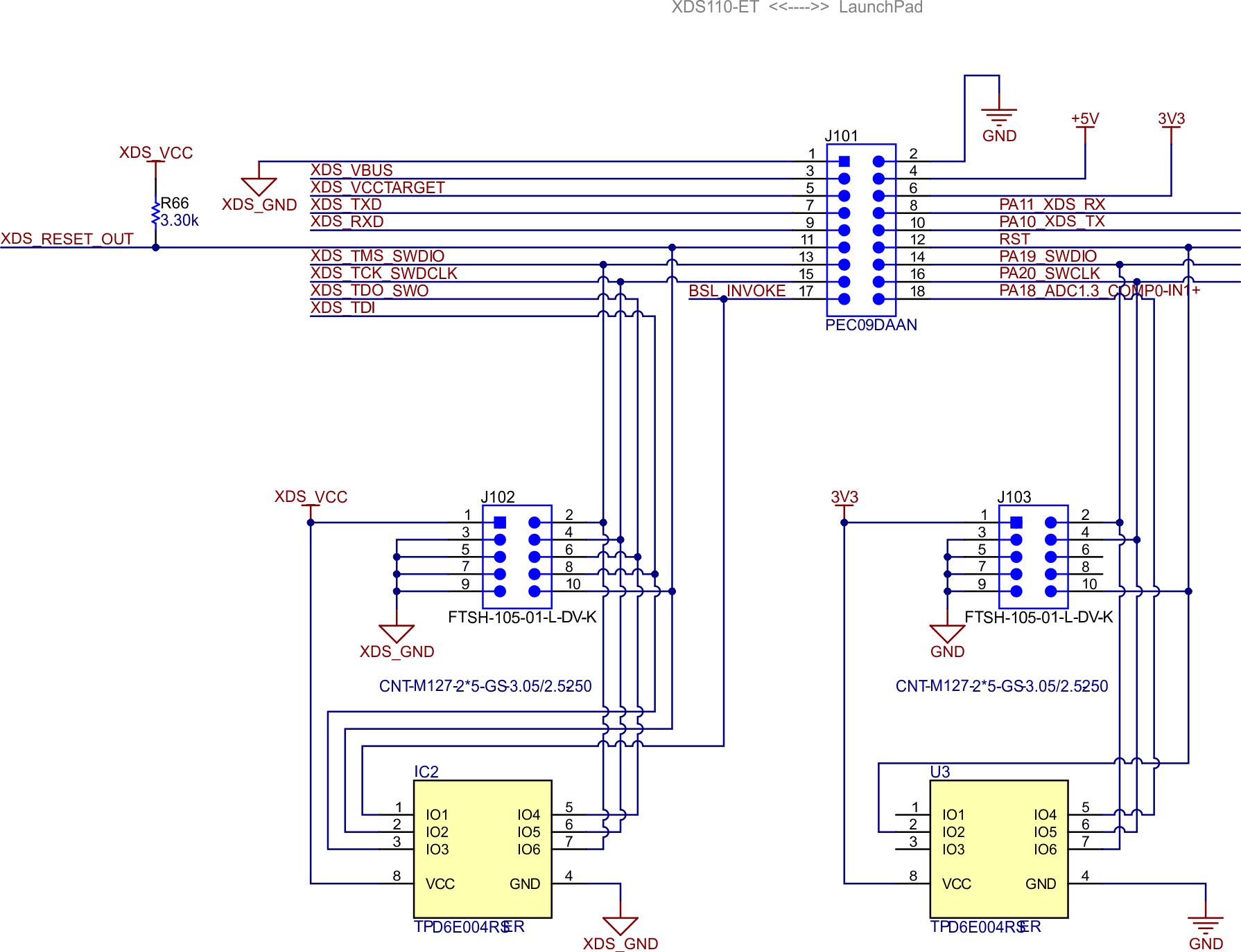
LP-MSPM0G3519 XDS110 Target Interface
                    Schematic Figure 4-5 XDS110 Target Interface Schematic
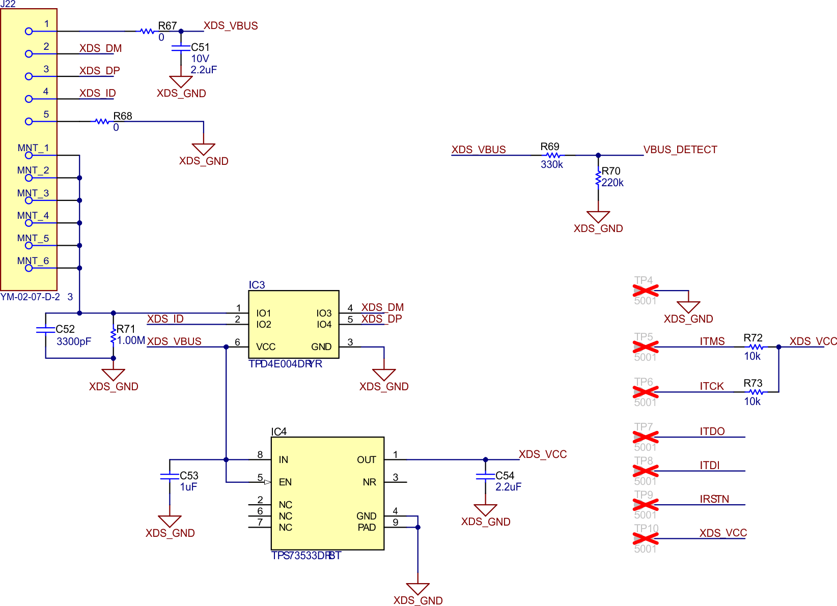
LP-MSPM0G3519 XDS110 USB Power
                    Schematic Figure 4-6 XDS110 USB Power Schematic
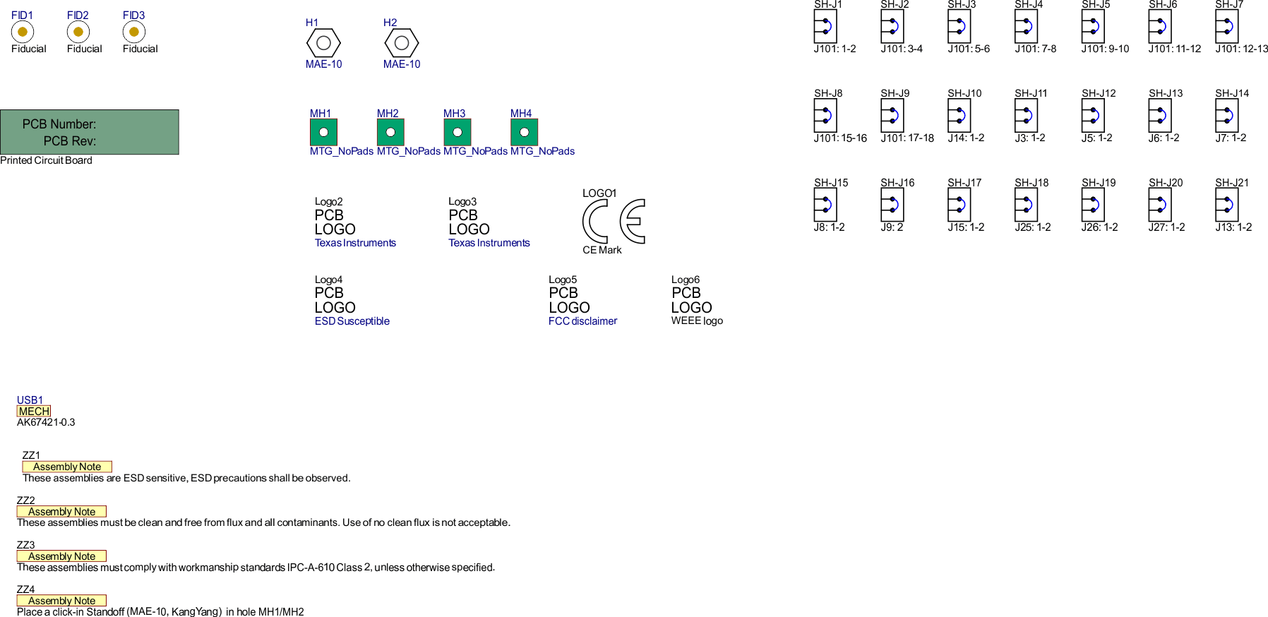
LP-MSPM0G3519 Jumpers and Standoffs Figure 4-7 Jumpers and Standoffs