-
PGA450Q1EVM-S User's Guide and TIDA-00151 UART Demo Instructional
PGA450Q1EVM-S User's Guide and TIDA-00151 UART Demo Instructional
PGA450Q1EVM-S User's Guide and TIDA-00151 UART Demo Instructional
The Texas Instruments PGA450-Q1 small form-factor evaluation module (EVM) allows users to evaluate the operation and performance of the PGA450-Q1 fully integrated system-on-chip analog front-end for ultrasonic sensing. The small form-factor layout of this EVM is equivalent to that of an end-product form factor, allowing users to easily integrate this PGA450-Q1-based sensor module into a real system without the need for additional prototypes.
Trademarks
All trademarks are the property of their respective owners.
1 Introduction
The PGA450Q1EVM-S is a fully assembled PCB design for real-world evaluation of the PGA450-Q1 ultrasonic-sensor signal-conditioner device, an ultrasonic transducer, and step-up transformer. This EVM can be integrated with systems for general object detection and distance measurement through air, in applications such as automotive park-assist, level sensing in tanks, collision avoidance for autonomous robotics, and unmanned aerial vehicle landing assist. This small form-factor EVM is intended to act as an ultrasonic module alternative to the full-scale PGA450Q1EVM. TI recommends that the user first begins evaluation with the PGA450Q1EVM before transitioning to evaluation with the PGA450Q1EVM-S.
2 Setup and Operation
This section describes how to setup and configure the PGA450Q1EVM-S for basic operation. A detailed description of connectors, jumpers, and test points are provided in addition to the typical operation setup of the EVM. An example of operation is also included.
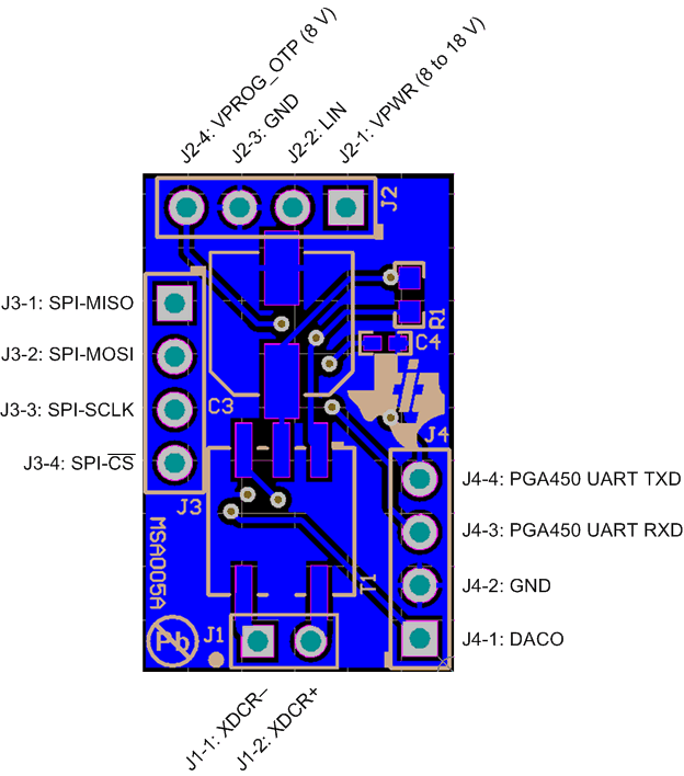
Figure 1 shows the PGA450Q1EVM-S pinout for the available input and output connectors.
 Figure 1. PGA460Q1EVM-S Pinout
 2.1 Input and Output Connectors
The PGA450Q1EVM-S has two power connectors, three communication interfaces, and two outputs. Table 1 lists the connectors in addition to a function description which includes the electrical specifications.
Table 1. Terminal Descriptors
| Terminal | Designator | Direction | Description |
|---|---|---|---|
| MAIN | J2-1 | Input | Single-system power supply to the VPWR pin of the PGA450-Q1 device. This supply is rated at 7 to 18 V DC for powering the entire board. |
| LIN | J2-2 | Input/Output | The PGA450-Q1 device implements the LIN 2.1 compliant physical layer. This physical layer can be used to communicate data between the PGA450-Q1 device and the master MCU. |
| GND | J2-3, J4-2 | — | Ground terminal to complete the circuit. |
| VPROG | J2-4 | Input | VPROG_OTP power supply input of 8 V for programming OTP memory of the PGA450-Q1 device. |
| SPI | J3 | Input/Output | SPI is the communication that is required for use with the PGA450Q1EVM GUI and TI GER USB interface for programming the PGA450-Q1 device(1). The internal 8051W must be placed in reset to communicate using SPI. |
| UART | J4-3, J4-4 | Input/Output | The TxD and RxD pins on the PGA450-Q1 device are connected to the 8051W UART. These two pins can be used either for software debugging or for implementing application-specific protocols. |
| DACO | J4-1 | Output | Observe the echo signal as an amplified analog signal or from a DAC output which converts a digitally filtered echo signal. In the Evaluation tab of the GUI, the quick-access buttons, Amplifier Output (unfiltered) and Datapath Output (filtered), are available. The signal is viewable on the DACO pin. Only one mode can be selected at a time. |
| XDCR Connector | J1 | Input/Output | The transducer (XDCR) connector is used to drive and listen for ultrasonic signals with an external transducer sensor element. |