SLDU019B December   2015  – March 2016 PGA450-Q1


  1.   PGA450Q1EVM-S User's Guide and TIDA-00151 UART Demo Instructional
    1.     Trademarks
    2. 1 Introduction
    3. 2 Setup and Operation
      1. 2.1 Input and Output Connectors
      2. 2.2 Basic Operation
        1. 2.2.1 Programming the PGA450-Q1 DEVRAM or OTP Memory
        2. 2.2.2 Programming the PGA450-Q1 EEPROM
        3. 2.2.3 Testing the UART Connection With the TI GER Board
      3. 2.3 UART Command Listing
    4. 3 Software
      1. 3.1 IDE Output File Configuration
        1. 3.1.1 Setup for DEVRAM Output File
        2. 3.1.2 Setup for OTP Output File
      2. 3.2 Interface Descriptions
        1. 3.2.1 UART Interface
        2. 3.2.2 LIN Interface
        3. 3.2.3 Serial-Peripheral Interface
    5. 4 Schematic, Bill of Materials, and Layout
      1. 4.1 Schematic
      2. 4.2 Bill of Materials
        1. 4.2.1 BOM
      3. 4.3 Board Layout and Component Placement
    6. 5 References
  2.   Revision History

Setup and Operation

This section describes how to setup and configure the PGA450Q1EVM-S for basic operation. A detailed description of connectors, jumpers, and test points are provided in addition to the typical operation setup of the EVM. An example of operation is also included.

Figure 1 shows the PGA450Q1EVM-S pinout for the available input and output connectors.
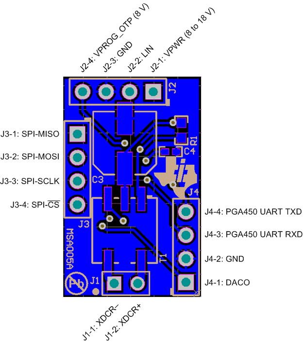
pinout_sldu019.gifFigure 1. PGA460Q1EVM-S Pinout