SLDU028A January 2018 – March 2020 TPS65313-Q1
-
TPS65313-EVM User’s Guide
- Trademarks
- 1 TPS65313-EVM Top View With Basic External Connections
- 2 TPS65313-EVM Input, Output Voltages, and Load Current Requirements
- 3 TPS65313-EVM Jumper Settings
- 4 TPS65313-EVM GUI Installing and Opening the GUI
- 5 TPS65313-EVM Power-Up and Power-Down Procedure
- 6 TPS65313 GUI
- 7 TPS65313-EVM Typical Plots
- 8 TPS65313-EVM Schematic Diagram
- 9 TPS65313-EVM Part List
- 10 PCB Layer Diagram
- 11 Description of the Watchdog Algorithm Implemented on EVM
- Revision History
7.6 Stability Measurements
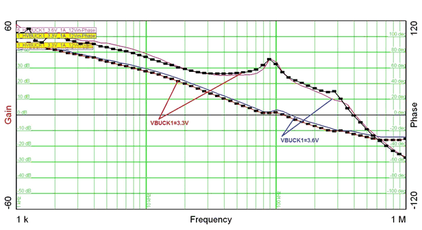
 Figure 30. BUCK1 Gain and Phase Plot With 1-A Load Current for VIN = 13 V
(Phase Margin ≈50 Degree, Bandwidth > 100 kHz)
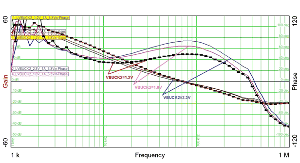
 Figure 31. BUCK2 Gain and Phase Plot With 1-A Load Current for VIN = 3.3 V
(Phase Margin >50 Degree, Bandwidth ≈75 kHz)
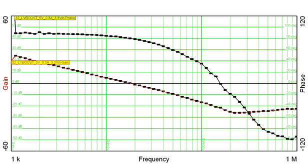
 Figure 32. BOOST Gain and Phase Plot With 0.3-A Load Current for VIN = 3.3 V
(Phase Margin >80 Degree, Bandwidth ≈20 kHz)