-
PCM1808 Single-Ended, Analog-Input 24-Bit, 96-kHz Stereo ADC
- 1 Features
- 2 Applications
- 3 Description
- 4 Revision History
- 5 Pin Configuration and Functions
- 6 Specifications
- 7 Detailed Description
- 8 Application and Implementation
- 9 Power Supply Recommendations
- 10Layout
- 11Device and Documentation Support
- 12Mechanical, Packaging, and Orderable Information
- IMPORTANT NOTICE
PCM1808 Single-Ended, Analog-Input 24-Bit, 96-kHz Stereo ADC
1 Features
- 24-Bit Delta-Sigma Stereo A/D Converter (ADC)
- Single-Ended Voltage Input: 3 Vp-p
- High Performance:
- THD+N: –93 dB (Typical)
- SNR: 99 dB (Typical)
- Dynamic Range: 99 dB (Typical)
- Oversampling Decimation Filter:
- Oversampling Frequency: ×64
- Pass-Band Ripple: ±0.05 dB
- Stop-Band Attenuation: –65 dB
- On-Chip High-Pass Filter: 0.91 Hz (48 kHz)
- Flexible PCM Audio Interface
- Master- or Slave-Mode Selectable
- Data Formats: 24-Bit I2S, 24-Bit Left-Justified
- Power Down and Reset by Halting System Clock
- Analog Antialias LPF Included
- Sampling Rate: 8 kHz–96 kHz
- System Clock: 256 fS, 384 fS, 512 fS
- Resolution: 24 Bits
- Dual Power Supplies:
- 5-V for Analog
- 3.3-V for Digital
- Package: 14-Pin TSSOP
2 Applications
- DVD Recorder
- Digital TV
- AV Amplifier or Receiver
- MD Player
- CD Recorder
- Multitrack Receiver
- Electric Musical Instrument
3 Description
The PCM1808 device is a high-performance, low-cost, single-chip, stereo analog-to-digital converter with single-ended analog voltage input. The PCM1808 device uses a delta-sigma modulator with 64-times oversampling and includes a digital decimation filter and high-pass filter that removes the dc component of the input signal. For various applications, the PCM1808 device supports master and slave mode and two data formats in serial audio interface.
The PCM1808 device supports the power-down and reset functions by means of halting the system clock.
The PCM1808 device is suitable for wide variety of cost-sensitive consumer applications requiring good performance and operation with a 5-V analog supply and 3.3-V digital supply. Fabrication of the PCM1808 device uses a highly advanced CMOS process. The device is available in a small, 14-pin TSSOP package.
Device Information(1)
| PART NUMBER | PACKAGE | BODY SIZE (NOM) |
|---|---|---|
| PCM1808 | TSSOP (14) | 4.40 mm × 5.00 mm |
- For all available packages, see the orderable addendum at the end of the datasheet.
PCM1808 Block Diagram

4 Revision History
Changes from A Revision (August 2006) to B Revision
- Added ESD Ratings table, Feature Description section, Device Functional Modes, Application and Implementation section, Power Supply Recommendations section, Layout section, Device and Documentation Support section, and Mechanical, Packaging, and Orderable Information section.Go
5 Pin Configuration and Functions

Pin Functions
| PIN | I/O | DESCRIPTION | |
|---|---|---|---|
| NAME | PIN | ||
| AGND | 2 | — | Analog GND |
| BCK | 8 | I/O | Audio-data bit-clock input or output (1) |
| DGND | 5 | — | Digital GND |
| DOUT | 9 | O | Audio-data digital output |
| FMT | 12 | I | Audio-interface format select (2) |
| LRCK | 7 | I/O | Audio-data latch-enable input or output (1) |
| MD0 | 10 | I | Audio-interface mode select 0 (2) |
| MD1 | 11 | I | Audio-interface mode select 1 (2) |
| SCKI | 6 | I | System clock input; 256 fS, 384 fS or 512 fS (3) |
| VCC | 3 | — | Analog power supply, 5-V |
| VDD | 4 | — | Digital power supply, 3.3-V |
| VINL | 13 | I | Analog input, L-channel |
| VINR | 14 | I | Analog input, R-channel |
| VREF | 1 | — | Reference-voltage decoupling (= 0.5 VCC) |
6 Specifications
6.1 Absolute Maximum Ratings
over operating ambient temperature range (unless otherwise noted) (1)| MIN | MAX | UNIT | |||
|---|---|---|---|---|---|
| VCC | Analog supply voltage | –0.3 | 6.5 | V | |
| VDD | Digital supply voltage | –0.3 | 4 | V | |
| Ground voltage differences | AGND, DGND | ±0.1 | V | ||
| Digital input voltage | LRCK, BCK, DOUT | –0.3 | (VDD + 0.3 V) < 4 | V | |
| SCKI, MD0, MD1, FMT | –0.3 | 6.5 | V | ||
| VINL, VINR, VREF | Analog input voltage | –0.3 | (VCC + 0.3 V) < 6.5 | V | |
| Input current (any pins except supplies) | ±10 | mA | |||
| TJ | Junction temperature | 150 | °C | ||
| Tstg | Storage temperature | –55 | 150 | °C | |
6.2 ESD Ratings
| VALUE | UNIT | |||
|---|---|---|---|---|
| V(ESD) | Electrostatic discharge | Human-body model (HBM), per ANSI/ESDA/JEDEC JS-001, all pins(1) | ±4000 | V |
| Charged-device model (CDM), per JEDEC specification JESD22-C101, all pins(2) | ±1500 | |||
6.3 Recommended Operating Conditions
over operating ambient temperature range (unless otherwise noted)| MIN | NOM | MAX | UNIT | |||
|---|---|---|---|---|---|---|
| VCC | Analog supply voltage (see Power Supply Recommendations) | 4.5 | 5 | 5.5 | V | |
| VDD | Digital supply voltage | 2.7 | 3.3 | 3.6 | V | |
| Analog input voltage, full scale (–0 dB) | VCC = 5 V | 3 | Vp-p | |||
| VIH (1) | High input logic level | 2 | VDD | VDC | ||
| VIL (1) | Low input logic level | 0 | 0.8 | VDC | ||
| VIH (2) (3) | High input logic level | 2 | 5.5 | VDC | ||
| VIL (2) (3) | Low input logic level | 0 | 0.8 | VDC | ||
| Digital input logic family | TTL compatible | |||||
| Digital input clock frequency, system clock | 2.048 | 49.152 | MHz | |||
| Digital input clock frequency, sampling clock | 8 | 96 | kHz | |||
| Digital output load capacitance | 20 | pF | ||||
| TA | Operating ambient temperature range | –40 | 85 | °C | ||
| TJ | Junction temperature | 150 | °C | |||
6.4 Thermal Information
| THERMAL METRIC(1) | PCM1808 | UNIT | |
|---|---|---|---|
| PW (TSSOP) | |||
| 14 PINS | |||
| RθJA | Junction-to-ambient thermal resistance | 89.4 | °C/W |
| RθJC(top) | Junction-to-case (top) thermal resistance | 25.6 | °C/W |
| RθJB | Junction-to-board thermal resistance | 30.3 | °C/W |
| ψJT | Junction-to-top characterization parameter | 1.4 | °C/W |
| ψJB | Junction-to-board characterization parameter | 29.8 | °C/W |
| RθJC(bot) | Junction-to-case (bottom) thermal resistance | N/A | °C/W |
6.5 Electrical Characteristics
All specifications at TA = 25°C, VCC = 5 V, VDD = 3.3 V, master mode, fS = 48 kHz, system clock = 512 fS, 24-bit data, unless otherwise noted| PARAMETER | TEST CONDITIONS | MIN | TYP | MAX | UNIT | |
|---|---|---|---|---|---|---|
| Resolution | 24 | Bits | ||||
| DATA FORMAT | ||||||
| Audio data interface format | I2S, left-justified | |||||
| Audio data bit length | 24 | Bits | ||||
| Audio data format | MSB-first, 2s complement | |||||
| fS | Sampling frequency | 8 | 48 | 96 | kHz | |
| System clock frequency | 256 fS | 2.048 | 12.288 | 24.576 | MHz | |
| 384 fS | 3.072 | 18.432 | 36.864 | |||
| 512 fS | 4.096 | 24.576 | 49.152 | |||
| INPUT LOGIC | ||||||
| VIH (1) | High input logic level | 2 | VDD | VDC | ||
| VIL (1) | Low input logic level | 0 | 0.8 | VDC | ||
| VIH (2) (3) | High input logic level | 2 | 5.5 | VDC | ||
| VIL (2) (3) | Low input logic level | 0 | 0.8 | VDC | ||
| IIH (2) | High input logic current | VIN = VDD | ±10 | µA | ||
| IIL (2) | Low input logic current | VIN = 0 V | ±10 | µA | ||
| IIH (1) (3) | High input logic current | VIN = VDD | 65 | 100 | µA | |
| IIL (1) (3) | Low input logic current | VIN = 0 V | ±10 | µA | ||
| OUTPUT LOGIC | ||||||
| VOH (4) | High output logic level | IOUT = –4 mA | 2.8 | VDC | ||
| VOL (4) | Low output logic level | IOUT = 4 mA | 0.5 | VDC | ||
| DC ACCURACY | ||||||
| Gain mismatch, channel-to-channel | ±1 | ±3 | % of FSR | |||
| Gain error | ±3 | ±6 | % of FSR | |||
| DYNAMIC PERFORMANCE (5) | ||||||
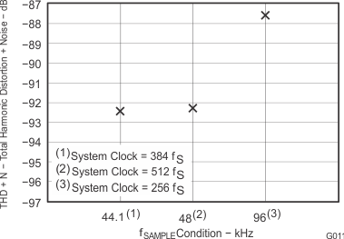
| THD+N | Total harmonic distortion + noise | VIN = –0.5 dB, fS = 48 kHz | –93 | –87 | dB | |
| VIN = –0.5 dB, fS = 96 kHz (6) | –87 | |||||
| VIN = –60 dB, fS = 48 kHz | –37 | |||||
| VIN = –60 dB, fS = 96 kHz (6) | –39 | |||||
| Dynamic range | fS = 48 kHz, A-weighted | 95 | 99 | dBVDC | ||
| fS = 96 kHz, A-weighted (6) | 101 | |||||
| S/N | Signal-to-noise ratio | fS = 48 kHz, A-weighted | 95 | 99 | dB | |
| fS = 96 kHz, A-weighted (6) | 101 | |||||
| Channel separation | fS = 48 kHz | 93 | 97 | dB | ||
| fS = 96 kHz (6) | 91 | |||||
| ANALOG INPUT | ||||||
| Input voltage | 0.6 VCC | Vp-p | ||||
| Center voltage (VREF) | 0.5 VCC | V | ||||
| Input impedance | 60 | kΩ | ||||
| Antialiasing filter frequency response | –3 dB | 1.3 | MHz | |||
| DIGITAL FILTER PERFORMANCE | ||||||
| Pass band | 0.454 fS | Hz | ||||
| Stop band | 0.583 fS | Hz | ||||
| Pass-band ripple | ±0.05 | dB | ||||
| Stop-band attenuation | –65 | dB | ||||
| Delay time | 17.4 / fS | |||||
| HPF frequency response | –3 dB | 0.019 fS / 1000 | ||||
| POWER SUPPLY REQUIREMENTS | ||||||
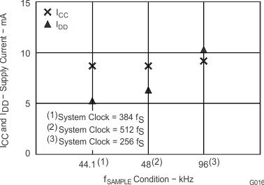
| ICC | Analog supply current (7) | fS = 48 kHz, 96 kHz (6) | 8.6 | 11 | mA | |
| Powered down (8) | 1 | μA | ||||
| IDD | Digital supply current (7) | fS = 48 kHz | 5.9 | 8 | mA | |
| fS = 96 kHz (6) | 10.2 | mA | ||||
| Powered down (8) | 150 | µA | ||||
| Power dissipation (7) | fS = 48 kHz | 62 | 81 | mW | ||
| fS = 96 kHz (6) | 77 | |||||
| Powered down (8) | 500 | µW | ||||
6.6 Timing Requirements
| MIN | NOM | MAX | UNIT | ||
|---|---|---|---|---|---|
| SYSTEM CLOCK TIMING | |||||
| tw(SCKH) | System clock pulse duration, HIGH | 8 | ns | ||
| tw(SCKL) | System clock pulse duration, LOW | 8 | ns | ||
| System clock duty cycle | 40% | 60% | |||
| CLOCK-HALT POWER-DOWN AND RESET TIMING | |||||
| t(CKR) | Delay time from SCKI halt to internal reset | 4 | µs | ||
| t(RST) | Delay time from SCKI resume to reset release | 1024 SCKI | µs | ||
| t(REL) | Delay time from reset release to DOUT output | 8960 / fS | µs | ||
| AUDIO DATA INTERFACE TIMING (Slave Mode: LRCK and BCK Work as Inputs)(1) | |||||
| t(BCKP) | BCK period | 1 / (64 fS) | ns | ||
| t(BCKH) | BCK pulse duration, HIGH | 1.5 × t(SCKI) | ns | ||
| t(BCKL) | BCK pulse duration, LOW | 1.5 × t(SCKI) | ns | ||
| t(LRSU) | LRCK setup time to BCK rising edge | 50 | ns | ||
| t(LRHD) | LRCK hold time to BCK rising edge | 10 | ns | ||
| t(LRCP) | LRCH period | 10 | µs | ||
| t(CKDO) | Delay time, BCK falling edge to DOUT valid | –10 | 40 | ns | |
| t(LRDO) | Delay time, LRCK edge to DOUT valid | –10 | 40 | ns | |
| tr | Rise time of all signals | 20 | ns | ||
| tf | Fall time of all signals | 20 | ns | ||
| AUDIO DATA INTERFACE TIMING (Master Mode: LRCK and BCK Work as Outputs)(2) | |||||
| t(BCKP) | BCK period | 150 | 1 / (64 fS) | 2000 | ns |
| t(BCKH) | BCK pulse duration, HIGH | 65 | 1200 | ns | |
| t(BCKL) | BCK pulse duration, LOW | 65 | 1200 | ns | |
| t(CKLR) | Delay time, BCK falling edge to LRCK valid | –10 | 20 | ns | |
| t(LRCP) | LRCK period | 10 | 1 / fS | 125 | ns |
| t(CKDO) | Delay time, BCK falling edge to DOUT valid | –10 | 20 | ns | |
| t(LRDO) | Delay time, LRCK edge to DOUT valid | –10 | 20 | ns | |
| tr | Rise time of all signals | 20 | ns | ||
| tf | Fall time of all signals | 20 | ns | ||
| AUDIO CLOCK INTERFACE TIMING (Master Mode: BCK Work as Outputs)(3) | |||||
| t(SCKBCK) | Delay time, SCKI rising edge to BCK edge | 5 | 30 | ns | |
 Figure 1. System Clock Timing
 Figure 2. Power-On Timing
 Figure 3. Clock-Halt Power-Down and Reset Timing
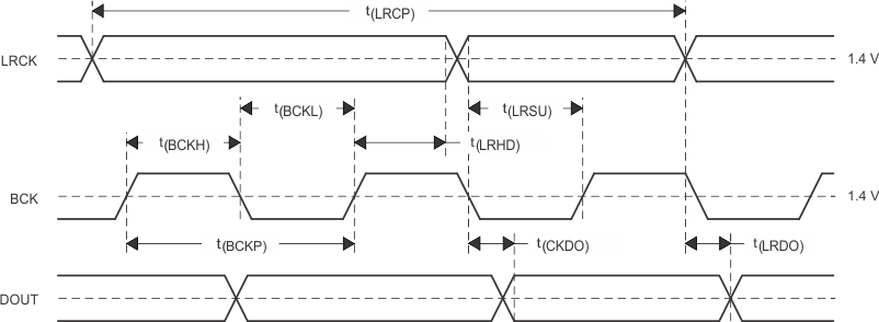 Figure 4. Audio Data Interface Timing (Slave Mode: LRCK and BCK Work as Inputs)
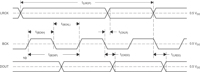 Figure 5. Audio Data Interface Timing (Master Mode: LRCK and BCK Work as Outputs)
 Figure 6. Audio Clock Interface Timing (Master Mode: BCK Works as Output)
6.7 Typical Characteristics
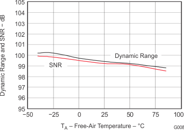
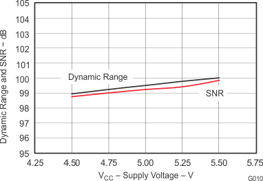
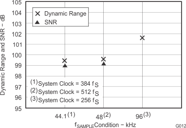
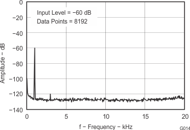
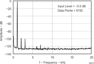
All specifications at TA = 25°C, VCC = 5 V, VDD = 3.3 V, master mode, fS = 48 kHz, system clock = 512 fS, 24-bit data, unless otherwise noted.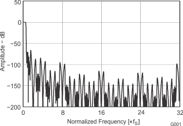
Overall Characteristics
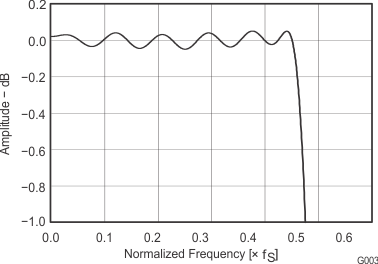
Pass-Band Ripple Characteristics
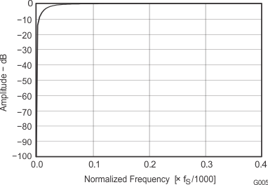
HPF Stop-Band Characteristics
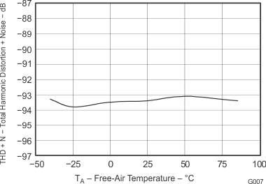
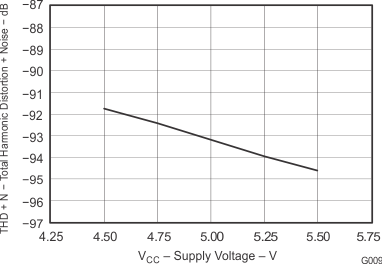
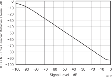
THD+N vs Signal Level
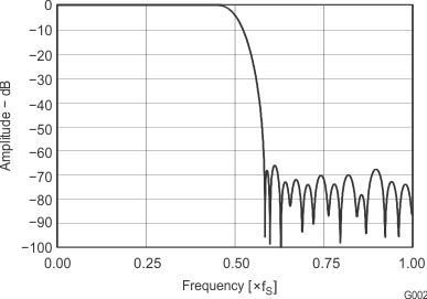
Stop-Band Attenuation Characteristics
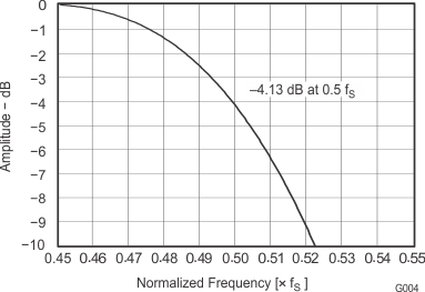
Transition-Band Characteristics
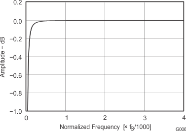
HPF Stop-Band Characteristics
