SLFS078C October   2006  – April 2024 TLC555-Q1

PRODUCTION DATA  

  1.   1
  2. Features
  3. Applications
  4. Description
  5. Pin Configuration and Functions
  6. Specifications
    1. 5.1 Absolute Maximum Ratings
    2. 5.2 ESD Ratings
    3. 5.3 Recommended Operating Conditions
    4. 5.4 Thermal Information
    5. 5.5 Electrical Characteristics: VDD = 5 V
    6. 5.6 Electrical Characteristics: VDD = 15 V
    7. 5.7 Switching Characteristics
    8. 5.8 Typical Characteristics
  7. Detailed Description
    1. 6.1 Overview
    2. 6.2 Functional Block Diagram
    3. 6.3 Feature Description
      1. 6.3.1 Monostable Operation
      2. 6.3.2 Astable Operation
      3. 6.3.3 Frequency Divider
    4. 6.4 Device Functional Modes
  8. Application and Implementation
    1. 7.1 Application Information
    2. 7.2 Typical Applications
      1. 7.2.1 Missing-Pulse Detector
        1. 7.2.1.1 Design Requirements
        2. 7.2.1.2 Detailed Design Procedure
        3. 7.2.1.3 Application Curve
      2. 7.2.2 Pulse-Width Modulation
        1. 7.2.2.1 Design Requirements
        2. 7.2.2.2 Detailed Design Procedure
        3. 7.2.2.3 Application Curve
      3. 7.2.3 Pulse-Position Modulation
        1. 7.2.3.1 Design Requirements
        2. 7.2.3.2 Detailed Design Procedure
        3. 7.2.3.3 Application Curve
      4. 7.2.4 Sequential Timer
        1. 7.2.4.1 Design Requirements
        2. 7.2.4.2 Detailed Design Procedure
        3. 7.2.4.3 Application Curve
    3. 7.3 Power Supply Recommendations
    4. 7.4 Layout
      1. 7.4.1 Layout Guidelines
      2. 7.4.2 Layout Example
  9. Device and Documentation Support
    1. 8.1 Documentation Support
      1. 8.1.1 Related Documentation
    2. 8.2 Receiving Notification of Documentation Updates
    3. 8.3 Support Resources
    4. 8.4 Trademarks
    5. 8.5 Electrostatic Discharge Caution
    6. 8.6 Glossary
  10. Revision History
  11. 10Mechanical, Packaging, and Orderable Information

Description

The TLC555-Q1 is a monolithic timing circuit fabricated using TI LinCMOS™ technology. The timer is fully compatible with CMOS, TTL, and MOS logic and operates at frequencies up to 2MHz. As a result of the high input impedance, this device supports smaller timing capacitors than capacitors used by the NE555. Thus, more accurate time delays and oscillations are possible. Power consumption is low across the full power-supply voltage range.

Like the NE555, the TLC555-Q1 has a trigger level equal to approximately one-third of the supply voltage, and a threshold level equal to approximately two-thirds of the supply voltage. These levels can be altered by using the control voltage pin (CONT). When the trigger input (TRIG) falls below the trigger level, the flip-flop is set, and the output goes high. If TRIG is greater than the trigger level and the threshold input (THRES) is greater than the threshold level, the flip-flop is reset and the output goes low. The reset input (RESET) can override all other inputs and is used to initiate a new timing cycle. If RESET is low, the flip-flop is reset and the output goes low. Whenever the output is low, a low-impedance path is provided between the discharge pin (DISCH) and GND. Tie all unused inputs to an appropriate logic level to prevent false triggering.
Package Information
PART NUMBER PACKAGE(1) PACKAGE SIZE(2)
TLC555-Q1 SOIC (8) 4.9mm × 6.0mm
For more information, see Section 10.
The package size (length × width) is a nominal value and includes pins, where applicable.


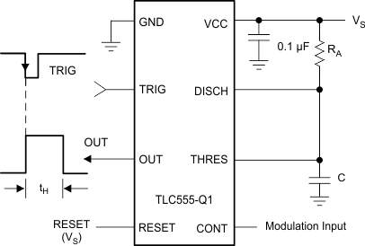
GUID-81DB7F7D-55BA-48A1-983D-4734563C55B9-low.gifPulse Width Modulator
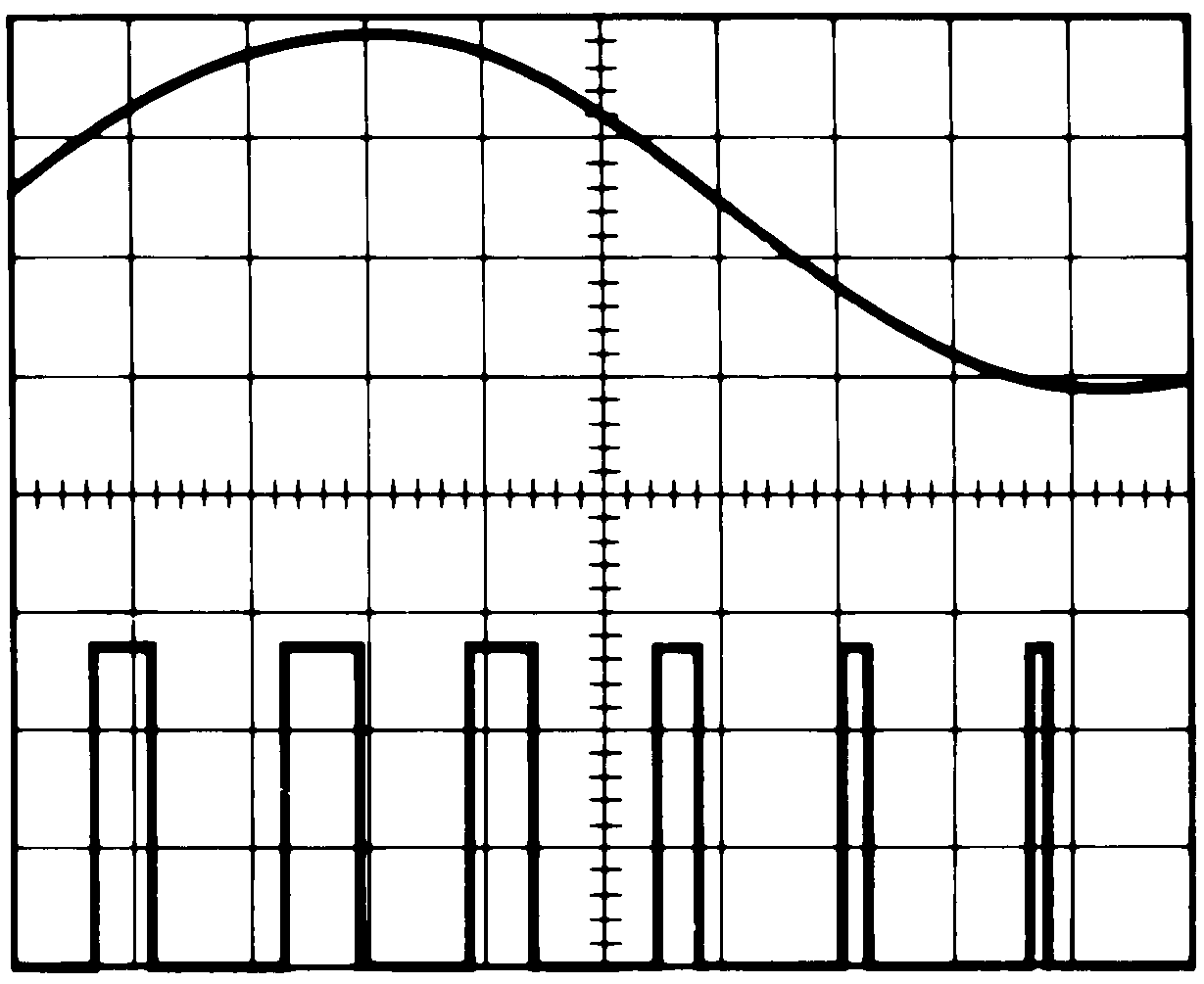
GUID-B32A1FEB-97B8-47E2-A31F-CB5B8F2056D5-low.pngPulse Width Modulator Waveform:
Top Waveform - Modulation
Bottom Waveform - Output Voltage