SLIA096 January 2022 DRV5021 , DRV5021-Q1 , DRV5023 , DRV5023-Q1 , DRV5032 , DRV5033 , DRV5033-Q1 , TMAG5123 , TMAG5123-Q1 , TMAG5124 , TMAG5124-Q1 , TMAG5131-Q1 , TMAG5231 , TMAG5328
2.7 Bench Results
After collecting all the data, assess whether the results make sense and possibly find explanations for inconsistencies. Ideally, all of the data falls within the expected measurement range based upon the threshold bounds calculated in the preliminary design phase. Such data could be assessed in a chart similar to Figure 2-20.
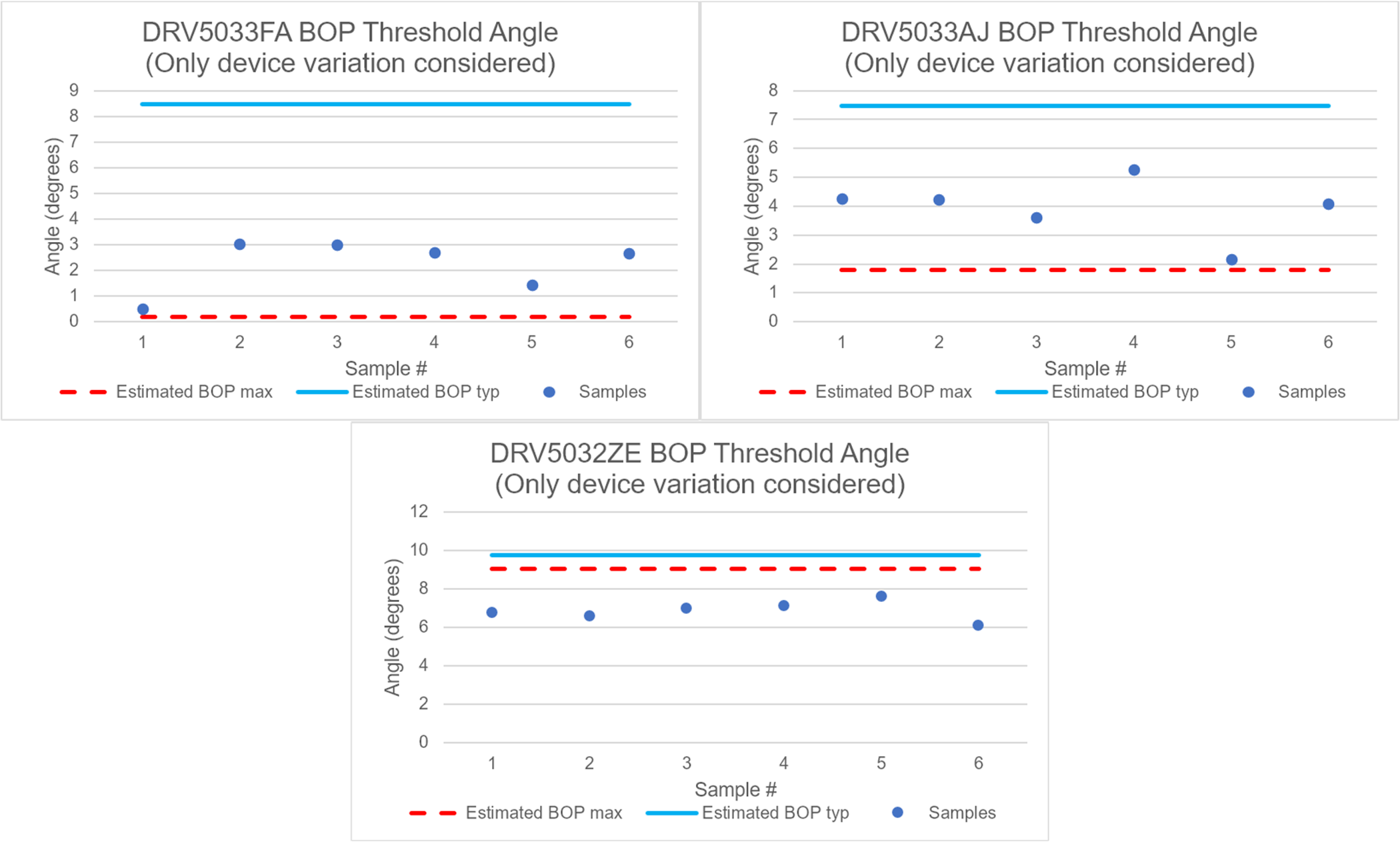
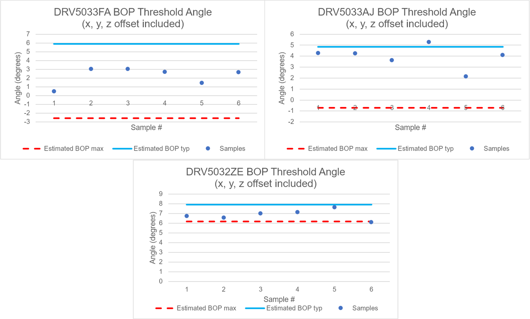
Figure 2-21 shows the results accumulated for three boards that each have one DRV5033FA-based rocker-switch, one DRV5033AJ-based rocker-switch, and one DRV5033ZE-based rocker-switch. Each rocker had two Hall-effect switches. Notice that some of the measured thresholds were not within the bounds suggested by the calculator tool. This is something to be expected when only Hall-effect switch variation and temperature drift is considered and the tolerances of the PCB and rocker switch structure have loose tolerances. After recalculating the BOP maximum threshold with some reasonable offset of 0.5 mm for x, y, and z included, notice that the measurements logged are not too unreasonable. The Error Sources section delves into the various error sources and attempts to quantify their impact.
 Figure 2-21 Bench Results vs Ideal Expectations
 Figure 2-22 Bench Results vs Bounds Including Offsets