SLIS150M March 2014 – June 2024 DRV5013
PRODUCTION DATA
- 1
- 1 Features
- 2 Applications
- 3 Description
- 4 Pin Configuration and Functions
- 5 Specifications
- 6 Detailed Description
- 7 Application and Implementation
- 8 Device and Documentation Support
- 9 Revision History
- 10Mechanical, Packaging, and Orderable Information
6.3.3 Power-On Time
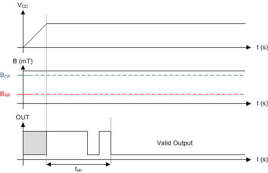
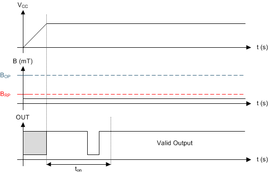
After applying VCC to the DRV5013 device, ton must elapse before the OUT pin is valid. During the power-up sequence, the output is Hi-Z. A pulse as shown in Figure 6-4 and Figure 6-5 occurs at the end of ton. This pulse can allow the host processor to determine when the DRV5013 output is valid after start-up. The power-up sequence, including the pulse, is the same for all device output versions (AD, AG, BC, FA, ND). Case 1, 2, 3 and 4 below show examples of valid outputs for the non-inverted output versions (AD, AG, BC, FA). In Case 1 (Figure 6-4) and Case 2 (Figure 6-5), the output is defined assuming a constant magnetic flux density B > BOP and B < BRP.
 Figure 6-4 Case 1: Power On When B >
BOP
 Figure 6-5 Case 2: Power On When B <
BRP
Figure 6-5 Case 2: Power On When B <
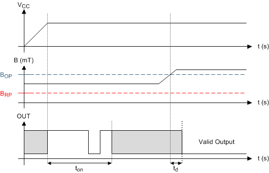
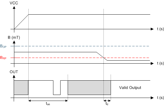
BRPIf the device is powered on with the magnetic flux density BRP < B < BOP, then the device output is indeterminate and can either be Hi-Z or pulled low. During the power-up sequence, the output is held Hi-Z until ton has elapsed. At the end of ton, a pulse is given on the OUT pin to indicate that ton has elapsed. After ton, if the magnetic flux density changes such that BOP < B, the output is released. Case 3 (Figure 6-6) and Case 4 (Figure 6-7) show examples of this behavior.
 Figure 6-6 Case 3: Power On When BRP
< B < BOP, Followed by B > BOP
 Figure 6-7 Case 4: Power On When BRP
< B < BOP, Followed by B < BRP