SLIS178B October   2017  – January 2018 TPS92830-Q1

PRODUCTION DATA.  

  1. Features
  2. Applications
  3. Description
    1.     Simplified Schematic
  4. Revision History
  5. Description (Continued)
  6. Pin Configuration and Functions
    1.     Pin Functions
  7. Specifications
    1. 7.1 Absolute Maximum Ratings
    2. 7.2 ESD Ratings
    3. 7.3 Recommended Operating Conditions
    4. 7.4 Thermal Information
    5. 7.5 Electrical Characteristics
    6. 7.6 Timing Requirements
    7. 7.7 Typical Characteristics
  8. Detailed Description
    1. 8.1 Overview
    2. 8.2 Functional Block Diagram
    3. 8.3 Feature Description
      1. 8.3.1 Device Bias
        1. 8.3.1.1 Power-On-Reset (POR)
        2. 8.3.1.2 Current Reference (IREF)
        3. 8.3.1.3 Low-Current Fault Mode
      2. 8.3.2 Charge Pump
        1. 8.3.2.1 Charge Pump Architecture
      3. 8.3.3 Constant-Current Driving
        1. 8.3.3.1 High-Side Current Sense
        2. 8.3.3.2 High-Side Current Driving
        3. 8.3.3.3 Gate Overdrive Voltage Protection
        4. 8.3.3.4 High-Precision Current Regulation
        5. 8.3.3.5 Parallel MOSFET Driving
      4. 8.3.4 PWM Dimming
        1. 8.3.4.1 Supply Dimming
        2. 8.3.4.2 PWM Dimming by Input
        3. 8.3.4.3 Internal Precision PWM Generator
        4. 8.3.4.4 Full Duty-Cycle Switch
      5. 8.3.5 Analog Dimming
        1. 8.3.5.1 Analog Dimming Topology
        2. 8.3.5.2 Internal High-Precision Pullup Current Source
      6. 8.3.6 Output Current Derating
        1. 8.3.6.1 Output-Current Derating Topology
      7. 8.3.7 Diagnostics and Fault
        1. 8.3.7.1 LED Short-to-GND Detection
        2. 8.3.7.2 LED Short-to-GND Auto Retry
        3. 8.3.7.3 LED Open-Circuit Detection
        4. 8.3.7.4 LED Open-Circuit Auto Retry
        5. 8.3.7.5 Dropout-Mode Diagnostics
        6. 8.3.7.6 Overtemperature Protection
        7. 8.3.7.7 FAULT Bus Output With One-Fails–All-Fail
        8. 8.3.7.8 Fault Table
    4. 8.4 Device Functional Modes
      1. 8.4.1 Undervoltage Lockout, V(IN) < V(UVLO)
      2. 8.4.2 Normal Operation (V(IN) ≥ 4.5 V, V(IN) > V(LED) + 0.5 V)
      3. 8.4.3 Low-Voltage Dropout
      4. 8.4.4 Fault Mode (Fault Is Detected)
  9. Application and Implementation
    1. 9.1 Application Information
    2. 9.2 Typical Applications
      1. 9.2.1 Typical Application for Automotive Exterior Lighting With One-Fails–All-Fail
        1. 9.2.1.1 Design Requirements
        2. 9.2.1.2 Detailed Design Procedure
        3. 9.2.1.3 Application Curves
      2. 9.2.2 High-Precision Dual-Brightness PWM Generation
        1. 9.2.2.1 Dual-Brightness Application
        2. 9.2.2.2 Design Requirements
        3. 9.2.2.3 Detailed Design Procedure
        4. 9.2.2.4 Application Curve
      3. 9.2.3 Driving High-Current LEDs With Parallel MOSFETs
        1. 9.2.3.1 Application Curves
  10. 10Layout
    1. 10.1 Layout Guidelines
    2. 10.2 Layout Example
  11. 11Device and Documentation Support
    1. 11.1 Receiving Notification of Documentation Updates
    2. 11.2 Community Resources
    3. 11.3 Trademarks
    4. 11.4 Electrostatic Discharge Caution
    5. 11.5 Glossary
  12. 12Mechanical, Packaging, and Orderable Information

Internal Precision PWM Generator

The TPS92830-Q1 device has an integrated precision PWM generator for on-chip PWM dimming as shown in . The device supports open-drain PWMOUT for synchronization between devices. Each device can be connected as a master, generating PWM, or as a slave, relying on external PWM sources. An external RC circuit precisely sets the duty cycle of the PWM generator across a wide duty-cycle range. Variation of the capacitor value affects the output frequency but not the duty cycle.

The PWM generator uses reference current 2 × I(IREF) as the internal charge current, I(PWMCHG).

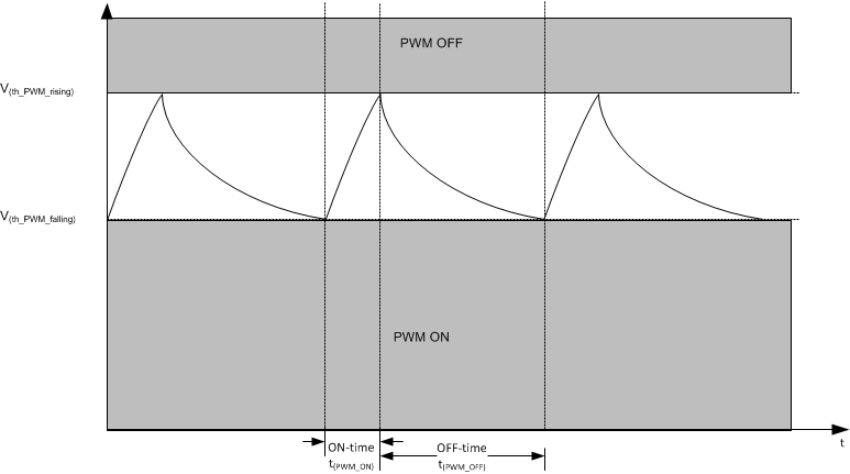
When V(PWMCHG) increases above rising threshold V(PWMCHG_th_rising), the constant-current source is turned off and V(PWMCHG) decays through the external resistor-capacitor circuit. The PWM output is set LOW. The PWMCHG threshold is set to V(PWMCHG_th_falling). When V(PWMCHG) decreases below falling threshold V(PWMCHG_th_falling), the constant-current source is turned on again to charge up the external capacitor. The PWM output is HIGH and the threshold is set to V(PWMCHG_th_rising).

TPS92830-Q1 Internal_PWM_Generator_with_Full_dutycycle_SLIS178.gifFigure 23. PWM Generator Dual-Brightness Configuration

An external resistor R(PWMEXT) and capacitor C(PWMEXT) are used to set the PWM cycle time.

Equation 3. TPS92830-Q1 Equation-pwm-ontime-slis178.gif
Equation 4. TPS92830-Q1 Equation-pwm-offtime-slis178.gif
Equation 5. TPS92830-Q1 Equation-pwm-freq-slis178.gif
Equation 6. TPS92830-Q1 Equation-pwm-dutycycle-slis178.gif
TPS92830-Q1 PWM_Dimming_Profile_SLIS178.gifFigure 24. PWM Dimming Profile