SLIU003A October 2009 – September 2022 TPS55065-Q1
3 Board Layout
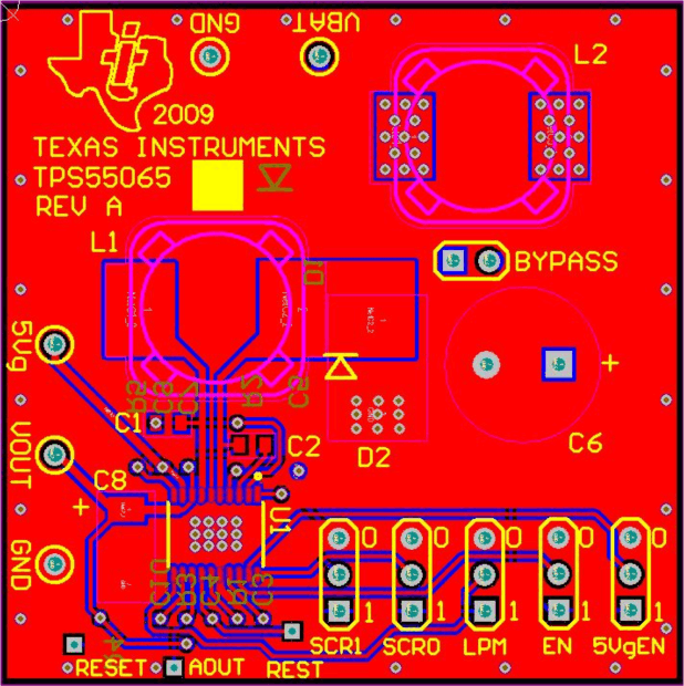
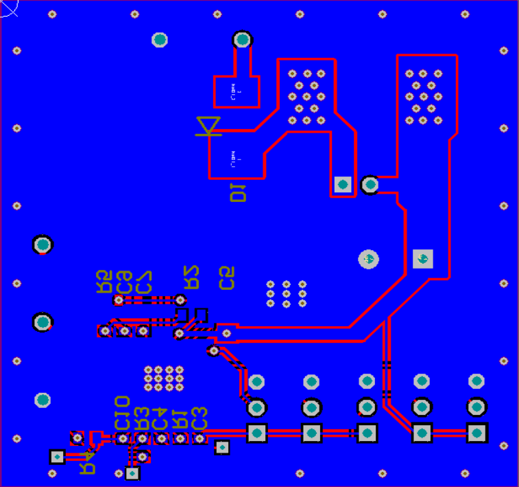
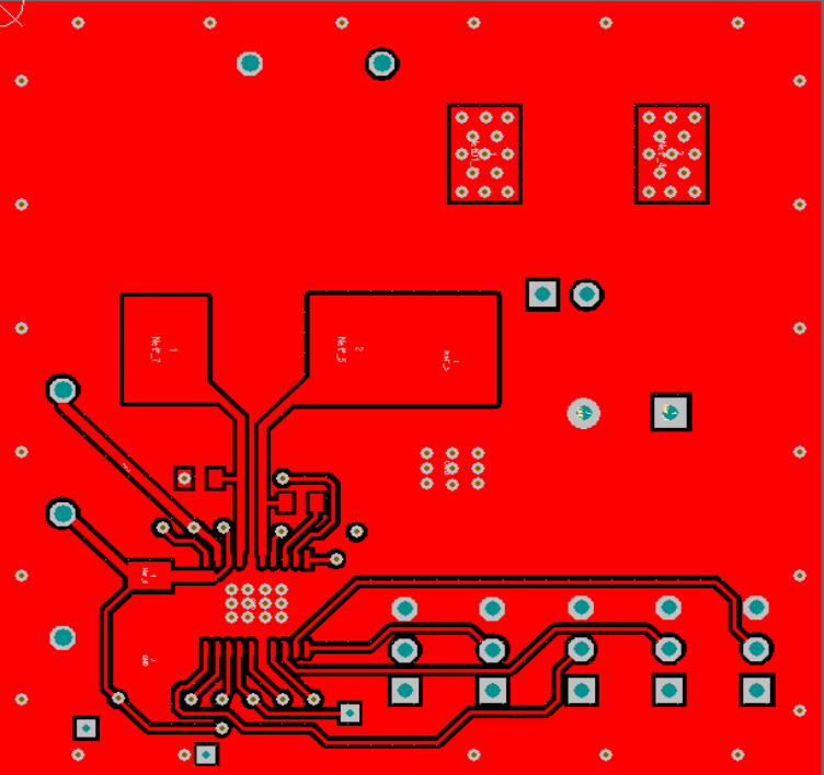
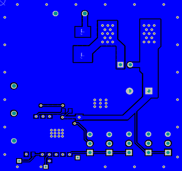
Figure 3-1, Figure 3-2, Figure 3-3, and Figure 3-4 show the board layout for the TPS55065EVM PWB. The EVM offers resistors, capacitors, and jumpers to program the switch pin slew rate and regulator turn-on Delay. Jumpers are also provided to enable the device and to enable the low-power mode option.
The TPS55065 offers high efficiency but does dissipate power. The PowerPAD™ package offers an exposed thermal pad to enhance thermal performance. This must be soldered to the copper landing on the PCB for optimal performance. The PCB provides 1-oz copper planes on the top and bottom to dissipate heat.
 Figure 3-1 Top Assembly Layer
 Figure 3-2 Bottom Assembly Layer
 Figure 3-3 Top Layer Routing
 Figure 3-4 Bottom Layer Routing