SLLA420C June 2018 – November 2024 ISO1211 , ISO1212 , ISO1228
1
Introduction
Digital input modules are frequently used in Programmable Logic Controllers (PLCs), Computer Numerical Control (CNC) and Railway Signaling Data Loggers, to detect 24V or higher voltage Digital Inputs (DI) from sensor transmitters. In some larger PLCs and Data Logger systems, more than 1000 digital inputs detection circuits need to be integrated in one board. Traditional Optocoupler designs (How To Simplify Isolated 24-V PLC Digital Input Module Designs) result in high board temperatures (heating up to 120℃ with ambient temp at 58℃), which can lead to reliability concerns. The implementation of high-wattage resistors and cooling fans to counter these temperatures add unneeded cost.
Industrial digital input modules usually use screw terminals to connect field sensors over long cables. This setup can pick up voltage and current noise from a variety of disturbances in harsh environments, such as surge, electrostatic discharge (ESD), and electrical fast transients (EFT). Surge can be caused by events such as lighting strikes. ESD can happen when a component or connector comes in contact with a human operator. EFT can be caused by cables near high-voltage and high-frequency signals.
Multichannel digital input boards are a growing trend. The efficient cost, compact size, and low-power dissipation encourage the growth of the trend. In this paper, techniques are introduced to optimize the space and thermal rise in the multichannel HV digital input board design. Other functionality and cost benefits are also presented.
Methods to Reduce Board Space
New Designs for Digital Input Modules
Texas Instruments' ISO1212 (2-channel) and ISO1228 (8-channel) devices provides a simple and low-power design with an accurate current limit to enable a more compact and high-density digital input board design. The current limit feature results in lower power dissipation, and lower board temperature rise, compared to traditional optocoupler based designs. These benefits are shown in this application brief, How To Simplify Isolated 24-V PLC Digital Input Module Designs. Two designs are shown here to detect bidirectional signal in the real PLC or CNC system. Figure 1(a) shows the use of two-channel digital input receivers with one COM terminal. Channel 1 and channel 2 are active when the digital input is sinking or sourcing respectively. But the state of the signal must be considered by the state of OUT1 and OUT2. This design consumes more microcontroller I/O pins and increase logic requirements. Figure 1(b) uses the rectifier followed by ISO1212 and can be used to detect two bidirectional signals for each device. For 'N-channel' digital input board design, the latter can save more PCB space and BOM cost for reducing usage of ‘N’ ISO1212s. The board can be more compact in America and Europe, where only unidirectional signals must be detected.
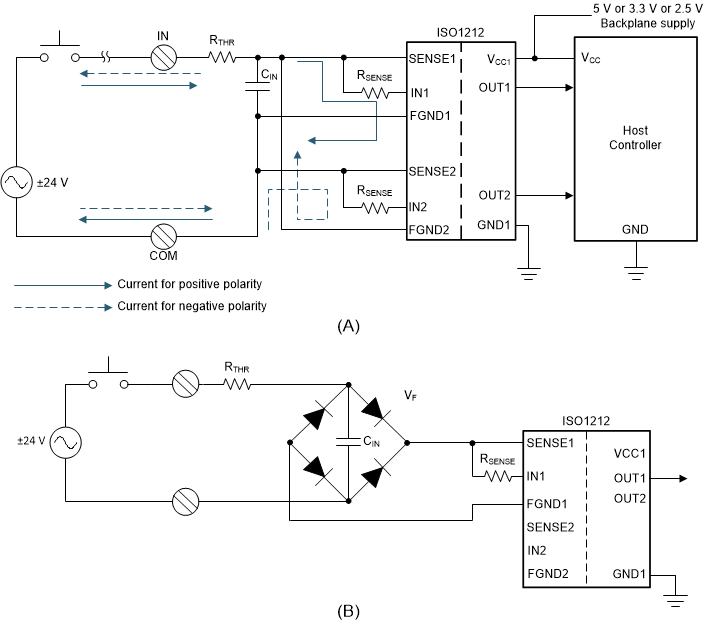 Figure 1 Two Designs for Bidirectional Signal Detection (a) ISO1212 With Sourcing and Sinking Input (b) ISO1212 With Bridge Rectifier
Use MUX and Decoder to Reduce the Total Number of Microcontroller I/O Pins
For an N-channel digital input board design in a large system, is impractical to use N Microcontroller I/Os to detect these signals. The ISO1212 provides an output-enable pin on the controller side (EN) to solve this. Setting the EN pin to 0 causes the output buffer to be in the high-impedance state. This feature can multiplex the ISO1212 on the controller side with external multiplexer and decoder.
Assuming that a 2 × N × M channel digital inputs board needs to be constructed; a block diagram of a digital input board system is shown in Figure 2. A module refers to the circuit chosen to detect bidirectional signals. The system is divided into M groups, and each group has the same output OUT1 to OUT2N, which saves (M-1) × N lines to a Micro. A multiplexer and decoder can be used to reduce more microcontroller I/Os when detecting the state of OUT1 and OUT2N. For example, a 16:1 MUX and 3-line to 8-line decoder can be used to detect 128 digital input signals while only using 8 I/O pins from the microcontroller. The usage of MUX, decoder and enable function of ISO1212 can be used to reduce the number of routed traces, which saves board space and reduce microcontroller I/O pin count.
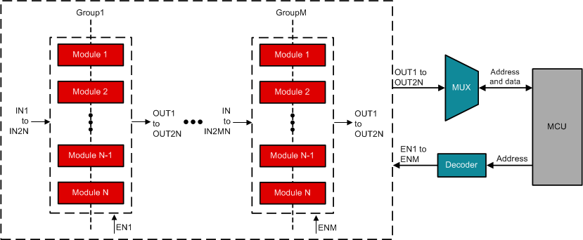 Figure 2 DI Board System Block Diagram
Layout Suggestions to Make the Board Compact
Use Symmetric Layout to Save Space
Use both the bottom and top layers to place the ISO1212 to realize a more compact board. The external spacing between the two sides that are being isolated must be maintained to pass safety standards. This distance is referred to as Clearance. The IEC 60950-1 is the primary standard describing the clearance requirement (ISO121x Isolated 24-V to 60-V Digital Input Receivers for Digital Input Modules). The shortest terminal-to-terminal distance through air of ISO1212 is 3.7mm. For some lower isolation voltage case, such as a PLC system, attain a minimum clearance no less than 3mm. Figure 3 shows the two different layout designs. Figure 3(a) shows the design using one side to place the connector, which makes the length of the board too long. The minimum clearance of the red and dark teal zone must be larger than 3.7mm. Figure 3(b) shows the design using two sides of the board to place the connector, the shape of this design is square. This design contains two distinct advantages: one is that this design is more common in most application, the other is that the design saves clearance between the field side and MCU side signal in the red and dark teal zone. One thing that must be carefully considered is that signal 1 in Figure 3(b) must be the MCU side signal. If field side signals are routed here, the 3mm clearance to the MCU connector increases.
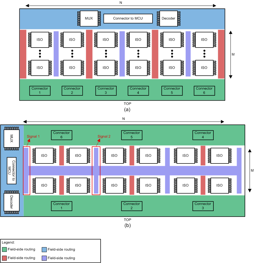 Figure 3 Two-Floor Design for Multichannel Digital Input Board Design (a) Using One Side to Place Connectors (b) Using Two Sides to Place Connectors
Reduce Decoupling Capacitor in the VCC1 Side
For most cases, a 100nF decoupling capacitor is required on VCC1 side. A decoupling capacitor is used to filter voltage noise and spikes that pass through DC signal. In some low speed multichannel digital input signal board design (switching frequency < 1kHz), some decoupling capacitors can be removed. For signal 2 in Figure 3(b), 2 × M pieces of ISO1212 are placed in the near zone. Only M pieces of ISO1212 are required for these 2M devices to filter and make the supply stable. M pieces of capacitor can be placed in the middle of this zone to make two side ISO1212 use the same capacitor, which can save the space of M times each capacitor size.
Use More Internal Layers When Routing the Signal
To make the board more compact, a multilayer board can be used to route the signals. Increase the use of internal layers to route the most signals, less signal routing in the top and bottom layers saves routing space. The internal spacing must be designed to meet some system level standard, such as IEC61010-1, which mandates a surge or impulse test for different isolation voltages. FR4 has a dielectric strength of 20kV/mm. So a 1mm minimum clearance between the field-side signal and MCU signal must be left to meet the surge voltage compliance. From this point, if more internal layers are used to route the signal, only 1mm clearance must be maintained, rather than 3mm in the top and bottom layers, thus the board is more compact.
Use Symmetric Layout When Routing the Signal
Utilize the top and bottom layers to place the ISO1212 to increase the channel density. Figure 4 shows the top view of ISO1212. To achieve good board density, make a specific layout of the top and bottom layers. Let the MCU signal side of the ISO1212 in the top layer have the same direction as the ISO1212 in the bottom layer. For example, Figure 5 shows the floor design of the multichannel board. Assume that N pieces of ISO1212 are controlled by the EN1 signal in the top layer, and N pieces of ISO1212 are controlled by the EN2 signal in the bottom layer. For the output signals that are multiplexed, some effort can be made to let the output signal of ISO1212 in the top layer (controlled by EN1) have the same position as the output signal of ISO1212 in the bottom layer (controlled by EN2). Now a via can be used to connect the same nets. The benefit of this symmetric routing is half of the output signal routing space can be saved by using vias.
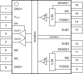 Figure 4 ISO1212 DBQ Package Top View
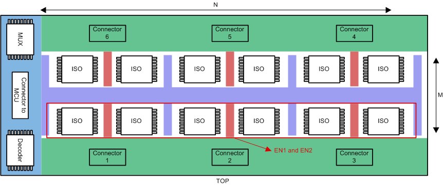 Figure 5 Multichannel DI Board Floor Plan Design
Conclusion
The ISO1212 (2-channel) and ISO1228 (8-channel)devices provides a simple and low-power design with an accurate current limit to enable a more compact and high-density digital input board design. The ISO1212 devices enable a more compact and high-density I/O module. The schematic and layout suggestions are introduced in this paper to make the digital input board more compact and meet the isolation compliance. Using different methods in different situations reduces more space in the board design.
Related Documentation
- Texas Instruments, How To Simplify Isolated 24-V PLC Digital Input Module Designsapplication brief.
- Texas Instruments, How to use isolation to improve ESD, EFT and surge immunity in industrial systems, analog applications journal
- David Lohbeck, Understanding isolator standards and certification to meet safety requirements, National Instruments, EDN, January 2016.
- Texas Instruments, ISO121x Isolated 24-V to 60-V Digital Input Receivers for Digital Input Modules, data sheet.
- Texas Instruments, Low-Emission Designs With ISOW7841 Integrated Signal and Power Isolator, application note.
| Device | Optimized Parameters | Performance Trade-Off |
|---|---|---|
| SN65HVS880 | 8-channel digital input serializer | Non-isolated, 3.6mA current limit, Needs field side supply |
| SN65HVS885 | 8-channel digital input serializer | Non-isolated, 3.6mA current limit, Needs isolated DC-DC |