SLLA595C march 2023 – june 2023 THVD1424 , THVD1454
- Abstract
- 2
- Trademarks
- 1Typical RS-485 Networks and the Need for Termination
- 2Network Length, Data Rate, and Stubs
- 3Discrete Design for Switchable Termination and Duplex Switching
- 4Discrete Design for Duplex Switching
- 5 THVD1424 and THVD1454 Flexible RS-485
- 6Application Diagrams with THVD1424
- 7Experimental Results from Four Node Testing of THVD1424
- 8Conclusion
- 9Revision History
6 Application Diagrams with THVD1424
Figure 6-1, Figure 6-2, and Figure 6-3 demonstrate the versatility of TI’s Flexible RS-485 transceiver, THVD1424. Network diagrams highlight how THVD1424 fits for both half-duplex and full-duplex networks. Same board design is replicated at all node positions with just software configuration. This also eliminates manual intervention for termination re-configuration as it can be handled by software.
 Figure 6-1 Half-duplex Network Using
THVD1424
 Figure 6-2 Full-duplex Network Using
THVD1424
Figure 6-2 Full-duplex Network Using
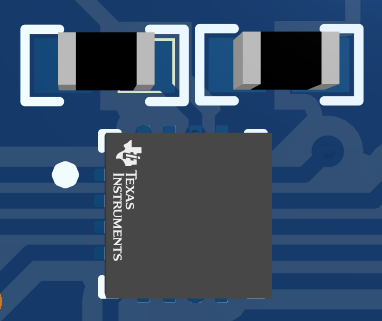
THVD1424THVD1424 only needs two 1 uF bypass capacitors on supply pins, VCC and VIO, to operate, thus providing an extremely compact feature-rich design. All logic pins can be hard-wired to supply or ground and are located in sides of the package. All four bus pins are located on one side of the package to enable a flow-through layout. Three-dimensional image of device with bypass capacitors is shown in Figure 6-3.
 Figure 6-3 Layout Diagram of
THVD1424