SLLA641 July 2024 TAA5212 , TAC5112 , TAC5212
2 ADC Front End Block Diagram
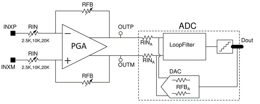
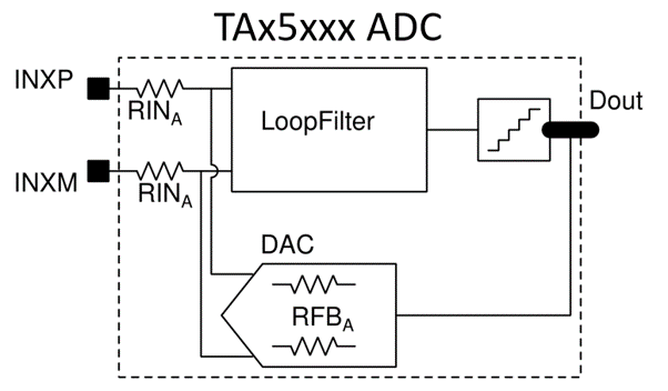
Here is a simplified block diagram of an ADC front-end of converter with PGA versus the TAX5XXX front-end which is without the PGA block. The difference is the PGA and ADC are now integrated and optimized in the new feedback DAC block of the new architecture.
The integration of the PGA on the new architecture is implemented in the DAC path of the ADC block. ADC front-end is a class B DAC, which behaves similar to PGA’s RFB block in Figure 2-1. The detail of the new RFB DAC architecture is not the scope of this application note.
 Figure 2-1 ADC Front-End With PGA
 Figure 2-2 ADC Front-End With PGA Integrated Into the ADC