SLLA643 August   2024 MCF8315C , MCF8315C-Q1 , MCF8316C-Q1


  1.   1
  2.   Abstract
  3.   Trademarks
  4. 1Introduction
  5. 2Power Pin Design Recommendations
    1. 2.1 VM
    2. 2.2 Charge Pump: CPH, CPL, CP
    3. 2.3 Buck Converter: FB_BK, SW_BK, GND_BK
    4. 2.4 AVDD
    5. 2.5 DVDD
    6. 2.6 PGND, AGND, DGND
    7. 2.7 Thermal Pad
  6. 3MCF831xC Buck Regulator Overview
    1. 3.1 Buck Regulator Mode of Operation
    2. 3.2 Buck Regulator Output Voltage
    3. 3.3 Buck Power Sequencing
    4. 3.4 Buck Inductor Selection
    5. 3.5 MCF831xC Operation Without Buck Regulator
  7. 4MCF831xC IO Pins Design Recommendations
    1. 4.1 SPEED Pin
    2. 4.2 BRAKE, DIR, DRVOFF pins
    3. 4.3 EXT_CLK, EXT_WD
    4. 4.4 ALARM
    5. 4.5 DACOUT1, DACOUT2
    6. 4.6 SDA, SCL
    7. 4.7 nFAULT and FG pin
  8. 5MCF831xC PCB Schematic and Layout Recommendations
    1. 5.1 Single Ground Plane
    2. 5.2 Single Ground with AVDD Shorted to FB_BK
    3. 5.3 Two Grounds
  9. 6Summary
  10. 7References

Two Grounds

For high performance applications, to avoid noise coupling between power and signal grounds, two ground planes can be used. Use one ground for AGND, DGND and GND_BK and another ground for PGND. Refer to Figure 5-5 and Figure 5-6 for a sample schematic and layout for a single ground plane PCB.
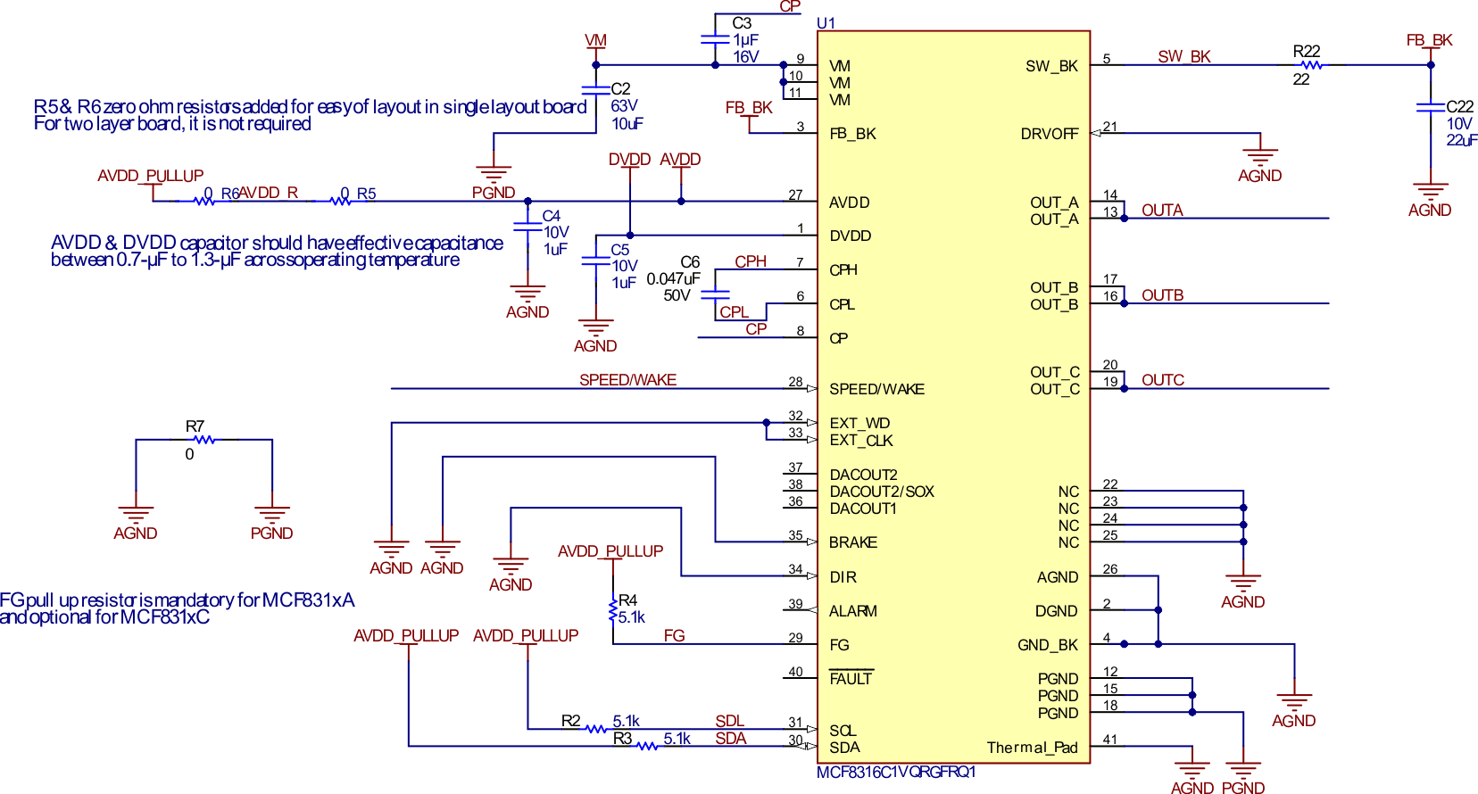
 PCB Schematic for Two Ground
                    Planes (AGND and PGND) Figure 5-5 PCB Schematic for Two Ground Planes (AGND and PGND)
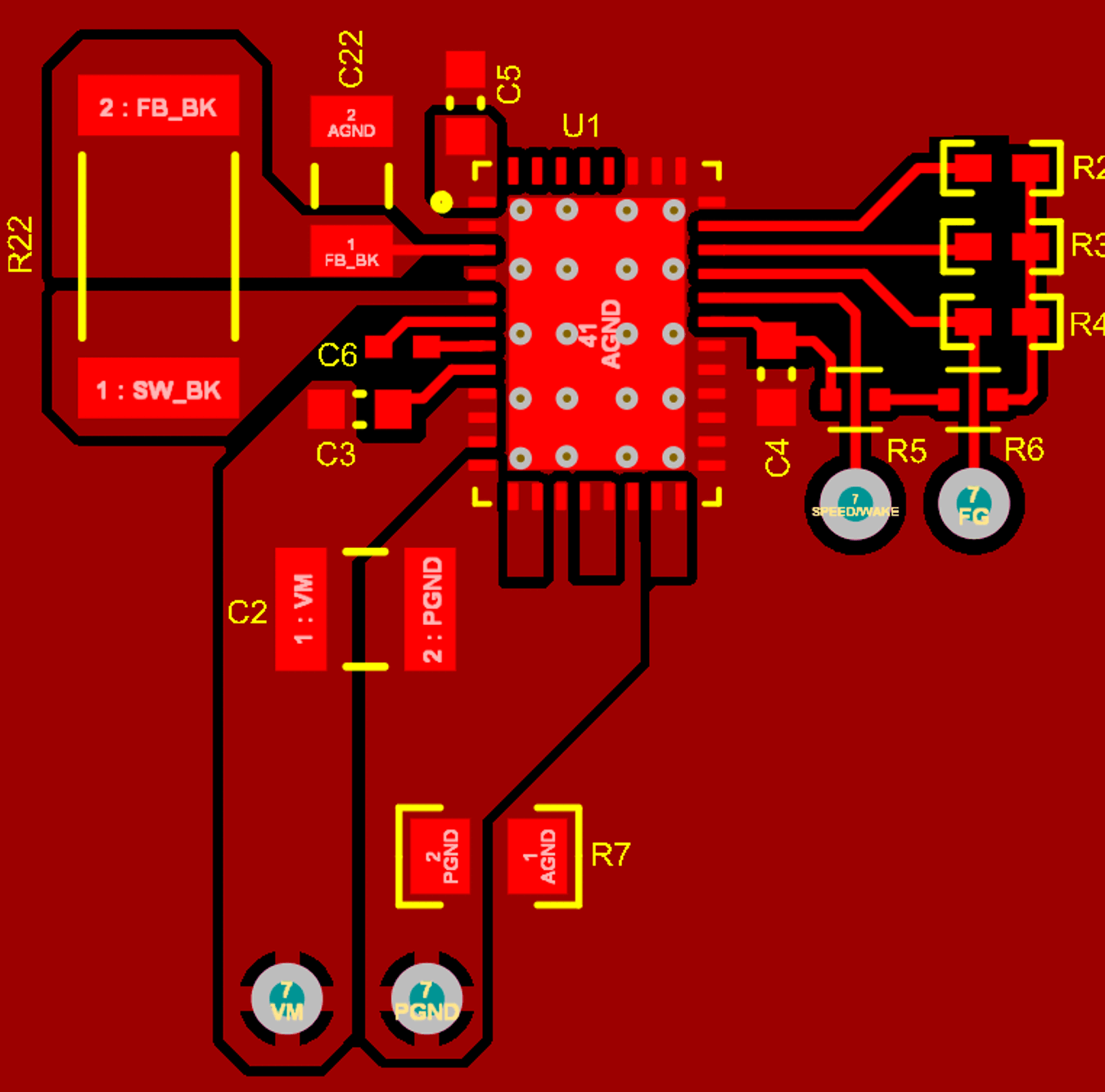
 PCB Layout for Two Ground
                    Planes (AGND and PGND) Figure 5-6 PCB Layout for Two Ground Planes (AGND and PGND)