SLLA643 August   2024 MCF8315C , MCF8315C-Q1 , MCF8316C-Q1


  1.   1
  2.   Abstract
  3.   Trademarks
  4. 1Introduction
  5. 2Power Pin Design Recommendations
    1. 2.1 VM
    2. 2.2 Charge Pump: CPH, CPL, CP
    3. 2.3 Buck Converter: FB_BK, SW_BK, GND_BK
    4. 2.4 AVDD
    5. 2.5 DVDD
    6. 2.6 PGND, AGND, DGND
    7. 2.7 Thermal Pad
  6. 3MCF831xC Buck Regulator Overview
    1. 3.1 Buck Regulator Mode of Operation
    2. 3.2 Buck Regulator Output Voltage
    3. 3.3 Buck Power Sequencing
    4. 3.4 Buck Inductor Selection
    5. 3.5 MCF831xC Operation Without Buck Regulator
  7. 4MCF831xC IO Pins Design Recommendations
    1. 4.1 SPEED Pin
    2. 4.2 BRAKE, DIR, DRVOFF pins
    3. 4.3 EXT_CLK, EXT_WD
    4. 4.4 ALARM
    5. 4.5 DACOUT1, DACOUT2
    6. 4.6 SDA, SCL
    7. 4.7 nFAULT and FG pin
  8. 5MCF831xC PCB Schematic and Layout Recommendations
    1. 5.1 Single Ground Plane
    2. 5.2 Single Ground with AVDD Shorted to FB_BK
    3. 5.3 Two Grounds
  9. 6Summary
  10. 7References

Single Ground Plane

For low cost applications, wherein switching noise coupling between power ground and signal ground is not critical, short all ground pins together. Refer to Figure 5-1 and Figure 5-2 for a sample schematic and layout for a single ground plane PCB.
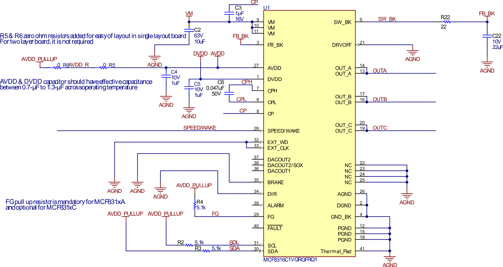
 PCB Schematic for Single
                    Ground Plane Figure 5-1 PCB Schematic for Single Ground Plane
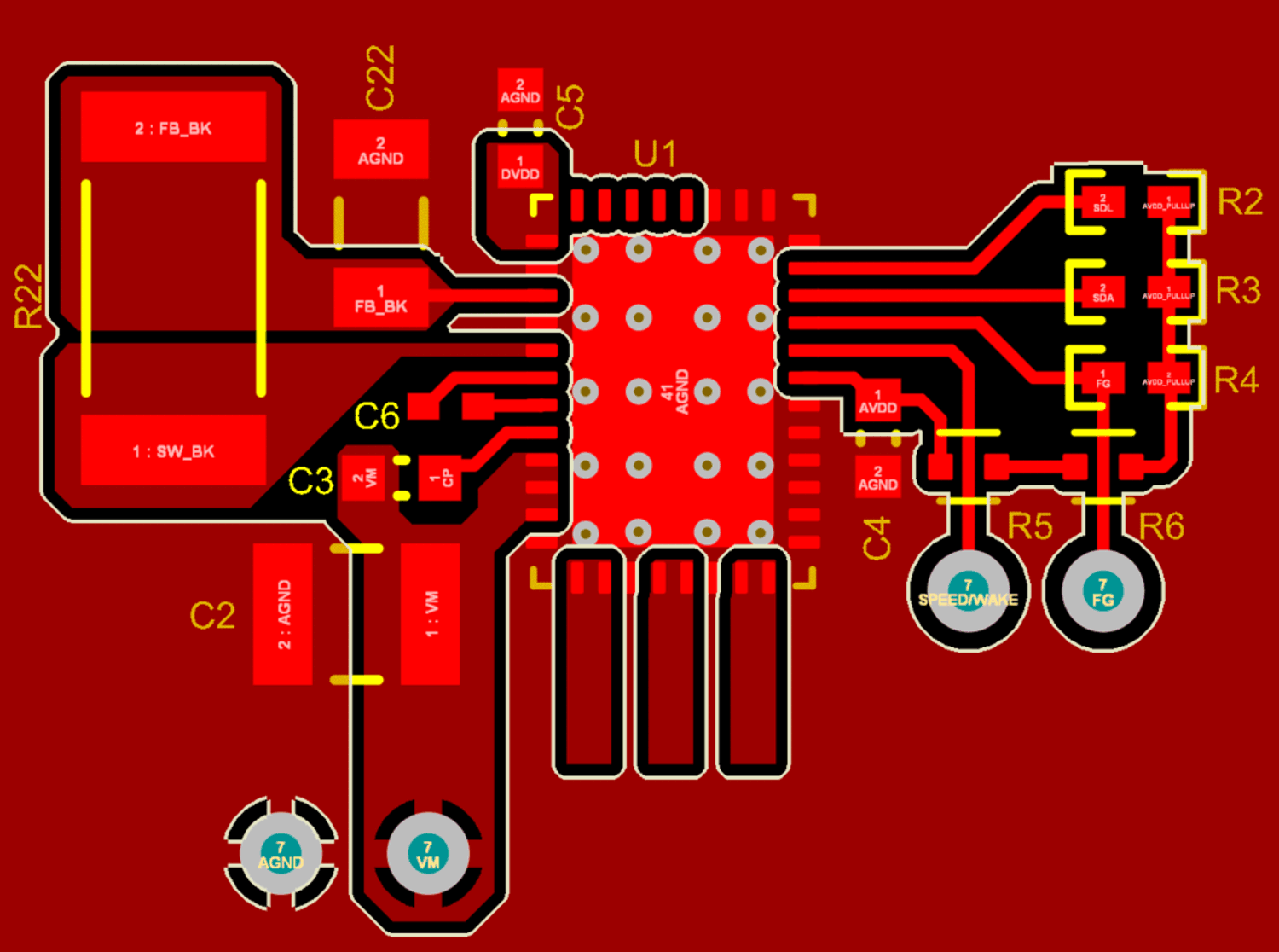
 PCB Layout for Single Ground
                    Plane Figure 5-2 PCB Layout for Single Ground Plane