SLLS373M July 1999 – March 2024 SN65LVDS1 , SN65LVDS2 , SN65LVDT2
PRODUCTION DATA
- 1
- 1 Features
- 2 Applications
- 3 Description
- 4 Device Options
- 5 Pin Configuration and Functions
- 6 Specifications
- 7 Parameter Measurement Information
- 8 Detailed Description
-
9 Application and Implementation
- 9.1 Application Information
- 9.2
Typical Applications
- 9.2.1
Point-to-Point Communications
- 9.2.1.1 Design Requirements
- 9.2.1.2
Detailed Design Procedure
- 9.2.1.2.1 Driver Supply Voltage
- 9.2.1.2.2 Driver Bypass Capacitance
- 9.2.1.2.3 Driver Input Voltage
- 9.2.1.2.4 Driver Output Voltage
- 9.2.1.2.5 Interconnecting Media
- 9.2.1.2.6 PCB Transmission Lines
- 9.2.1.2.7 Termination Resistor
- 9.2.1.2.8 Driver NC Pins
- 9.2.1.2.9 Receiver Supply Voltage
- 9.2.1.2.10 Receiver Bypass Capacitance
- 9.2.1.2.11 Receiver Input Common-Mode Range
- 9.2.1.2.12 Receiver Input Signal
- 9.2.1.2.13 Receiver Output Signal
- 9.2.1.2.14 Receiver NC Pins
- 9.2.2 Application Curve
- 9.2.3 Multidrop Communications
- 9.2.1
Point-to-Point Communications
- 10Power Supply Recommendations
- 11Layout
- 12Device and Documentation Support
- 13Revision History
- 14Mechanical, Packaging, and Orderable Information
8.3.2.5 Receiver Equivalent Schematics
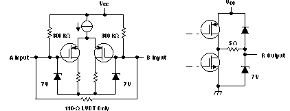
The SN65LVDS2 and SN65LVDT2 equivalent input and output schematic diagrams are shown in Figure 8-3. The receiver input is a high-impedance differential pair in the case of the SN65LVDS2. The SN65LVDT2 includes an internal termination resistor of 110 Ω across the input port. 7-V Zener diodes are included on each input to provide ESD protection. The receiver output structure shown is a CMOS inverter with an additional Zener diode, again for ESD protection.
 Figure 8-3 Receiver Equivalent Input and Output Schematic Diagrams