SLLS573E December 2003 – March 2024 SN65MLVD200A , SN65MLVD202A , SN65MLVD204A , SN65MLVD205A
PRODUCTION DATA
- 1
- 1 Features
- 2 Applications
- 3 Description
- 4 Device Comparison Table
- 5 Pin Configuration and Functions
-
6 Specifications
- 6.1 Absolute Maximum Ratings
- 6.2 ESD Ratings
- 6.3 Recommended Operating Conditions
- 6.4 Thermal Information
- 6.5 Electrical Characteristics
- 6.6 Electrical Characteristics – Driver
- 6.7 Electrical Characteristics – Receiver
- 6.8 Electrical Characteristics – BUS Input and Output
- 6.9 Switching Characteristics – Driver
- 6.10 Switching Characteristics – Receiver
- 6.11 Typical Characteristics
- 7 Parameter Measurement Information
- 8 Detailed Description
-
9 Application and Implementation
- 9.1 Application Information
- 9.2
Typical Application
- 9.2.1 Design Requirements
- 9.2.2
Detailed Design Procedure
- 9.2.2.1 Supply Voltage
- 9.2.2.2 Supply Bypass Capacitance
- 9.2.2.3 Driver Input Voltage
- 9.2.2.4 Driver Output Voltage
- 9.2.2.5 Termination Resistors
- 9.2.2.6 Receiver Input Signal
- 9.2.2.7 Receiver Input Threshold (Failsafe)
- 9.2.2.8 Receiver Output Signal
- 9.2.2.9 Interconnecting Media
- 9.2.2.10 PCB Transmission Lines
- 9.2.3 Application Curves
- 10Power Supply Recommendations
- 11Layout
- 12Device and Documentation Support
- 13Revision History
- 14Mechanical, Packaging, and Orderable Information
11.1.1 Microstrip Versus Stripline Topologies
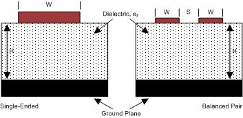
According to the LVDS Application and Data Handbook (SLLD009), printed-circuit boards usually offer designers two transmission line options: microstrip and stripline. Microstrips are traces on the outer layer of a PCB, as shown in Figure 11-1.
 Figure 11-1 Microstrip Topology
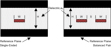
Striplines are traces between two ground planes (see Figure 11-2). Striplines are less prone to emissions and susceptibility problems because the reference planes effectively shield the embedded traces. However, from the standpoint of high-speed transmission, juxtaposing two planes creates additional capacitance. TI recommends routing M-LVDS signals on microstrip transmission lines if possible. The PCB traces allow designers to specify the necessary tolerances for ZO based on the overall noise budget and reflection allowances. Footnotes 11, 22, and 33 provide the documentation for formulas for ZO and tPD for differential and single-ended traces. (2)(3)(4)
 Figure 11-2 Stripline Topology