SLLS573E December 2003 – March 2024 SN65MLVD200A , SN65MLVD202A , SN65MLVD204A , SN65MLVD205A
PRODUCTION DATA
- 1
- 1 Features
- 2 Applications
- 3 Description
- 4 Device Comparison Table
- 5 Pin Configuration and Functions
-
6 Specifications
- 6.1 Absolute Maximum Ratings
- 6.2 ESD Ratings
- 6.3 Recommended Operating Conditions
- 6.4 Thermal Information
- 6.5 Electrical Characteristics
- 6.6 Electrical Characteristics – Driver
- 6.7 Electrical Characteristics – Receiver
- 6.8 Electrical Characteristics – BUS Input and Output
- 6.9 Switching Characteristics – Driver
- 6.10 Switching Characteristics – Receiver
- 6.11 Typical Characteristics
- 7 Parameter Measurement Information
- 8 Detailed Description
-
9 Application and Implementation
- 9.1 Application Information
- 9.2
Typical Application
- 9.2.1 Design Requirements
- 9.2.2
Detailed Design Procedure
- 9.2.2.1 Supply Voltage
- 9.2.2.2 Supply Bypass Capacitance
- 9.2.2.3 Driver Input Voltage
- 9.2.2.4 Driver Output Voltage
- 9.2.2.5 Termination Resistors
- 9.2.2.6 Receiver Input Signal
- 9.2.2.7 Receiver Input Threshold (Failsafe)
- 9.2.2.8 Receiver Output Signal
- 9.2.2.9 Interconnecting Media
- 9.2.2.10 PCB Transmission Lines
- 9.2.3 Application Curves
- 10Power Supply Recommendations
- 11Layout
- 12Device and Documentation Support
- 13Revision History
- 14Mechanical, Packaging, and Orderable Information
3 Description
The SN65MLVD20xx devices are multipoint low-voltage differential (M-LVDS) line drivers and receivers that are optimized to operate at signaling rates up to 100 Mbps. All parts comply with the multipoint low-voltage differential signaling (M-LVDS) standard TIA/EIA-899.
The SN65MLVD20xx devices have enhancements over their predecessors. Improved features include controlled slew rate on the driver output to help minimize reflections from unterminated stubs, which results in better signal integrity. Additionally, 8-kV ESD protection on the bus pins for more robustness. The same footprint definition was maintained making for an easy drop-in replacement for a system performance upgrade.
The devices are characterized for operation from –40°C to 85°C.
| PART NUMBER | PACKAGE(1) | BODY SIZE (NOM) |
|---|---|---|
| SN65MLVD200A | SOIC (8) | 4.90 mm × 3.91 mm |
| SN65MLVD204A | ||
| SN65MLVD202A | SOIC (14) | 8.65 mm × 3.91 mm |
| SN65MLVD205A |
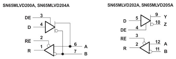
 Logic Diagrams (Positive
Logic)