SLLS573E December 2003 – March 2024 SN65MLVD200A , SN65MLVD202A , SN65MLVD204A , SN65MLVD205A
PRODUCTION DATA
- 1
- 1 Features
- 2 Applications
- 3 Description
- 4 Device Comparison Table
- 5 Pin Configuration and Functions
-
6 Specifications
- 6.1 Absolute Maximum Ratings
- 6.2 ESD Ratings
- 6.3 Recommended Operating Conditions
- 6.4 Thermal Information
- 6.5 Electrical Characteristics
- 6.6 Electrical Characteristics – Driver
- 6.7 Electrical Characteristics – Receiver
- 6.8 Electrical Characteristics – BUS Input and Output
- 6.9 Switching Characteristics – Driver
- 6.10 Switching Characteristics – Receiver
- 6.11 Typical Characteristics
- 7 Parameter Measurement Information
- 8 Detailed Description
-
9 Application and Implementation
- 9.1 Application Information
- 9.2
Typical Application
- 9.2.1 Design Requirements
- 9.2.2
Detailed Design Procedure
- 9.2.2.1 Supply Voltage
- 9.2.2.2 Supply Bypass Capacitance
- 9.2.2.3 Driver Input Voltage
- 9.2.2.4 Driver Output Voltage
- 9.2.2.5 Termination Resistors
- 9.2.2.6 Receiver Input Signal
- 9.2.2.7 Receiver Input Threshold (Failsafe)
- 9.2.2.8 Receiver Output Signal
- 9.2.2.9 Interconnecting Media
- 9.2.2.10 PCB Transmission Lines
- 9.2.3 Application Curves
- 10Power Supply Recommendations
- 11Layout
- 12Device and Documentation Support
- 13Revision History
- 14Mechanical, Packaging, and Orderable Information
7 Parameter Measurement Information
 Figure 7-1 Driver
Voltage and Current Definitions
A. All resistors are 1%
tolerance.
Figure 7-2 Differential Output Voltage Test Circuit
A. All input pulses are supplied by a
generator having the following characteristics: tr or tf≤
1 ns, pulse frequency = 1 MHz, duty cycle = 50 ± 5%.
B. C1, C2 and C3 include
instrumentation and fixture capacitance within 2 cm of the D.U.T. and are
±20%.
C. R1 and R2 are metal film, surface
mount, ±1%, and located within 2 cm of the D.U.T.
D. The measurement of
VOS(PP) is made on test equipment with a –3 dB bandwidth of at
least 1 GHz.
Figure 7-3 Test
Circuit and Definitions for the Driver Common-Mode Output Voltage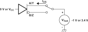 Figure 7-4 Driver
Short-Circuit Test Circuit
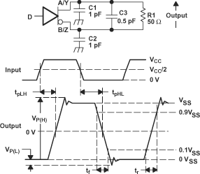
A. All input pulses are supplied by a
generator having the following characteristics: tr or tf≤
1 ns, frequency = 1 MHz, duty cycle = 50 ± 5%.
B. C1, C2, and C3 include
instrumentation and fixture capacitance within 2 cm of the D.U.T. and are
±20%.
C. R1 is a metal film, surface mount,
and 1% tolerance and located within 2 cm of the D.U.T.
D. The measurement is made on test
equipment with a –3 dB bandwidth of at least 1 GHz.
Figure 7-5 Driver
Test Circuit, Timing, and Voltage Definitions for the Differential Output
Signal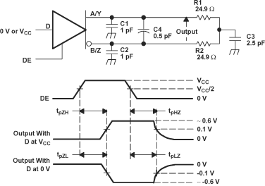
A. All input pulses are supplied by a
generator having the following characteristics: tr or tf≤
1 ns, frequency = 1 MHz, duty cycle = 50 ± 5%.
B. C1, C2, C3, and C4 includes
instrumentation and fixture capacitance within 2 cm of the D.U.T. and are
±20%.
C. R1 and R2 are metal film, surface
mount, and 1% tolerance and located within 2 cm of the D.U.T.
D. The measurement is made on test
equipment with a –3 dB bandwidth of at least 1 GHz.
Figure 7-6 Driver
Enable and Disable Time Circuit and Definitions Figure 7-7 Maximum
Steady State Output Voltage
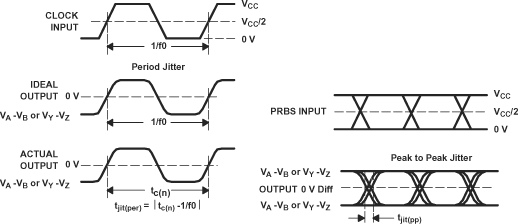
A. All input pulses are supplied by an
Agilent 81250 Stimulus System.
B. The measurement is made on a TEK
TDS6604 running TDSJIT3 application software
C. Period jitter is measured using a 50
MHz 50 ±1% duty cycle clock input.
D. Peak-to-peak jitter is measured
using a 100 Mbps 215 –1 PRBS input.
Figure 7-8 Driver
Jitter Measurement Waveforms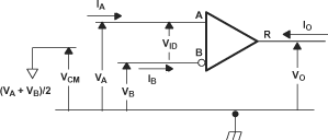 Figure 7-9 Receiver
Voltage and Current Definitions
Figure 7-9 Receiver
Voltage and Current DefinitionsTable 7-1 Type-1
Receiver Input Threshold Test Voltages
| APPLIED VOLTAGES | RESULTING DIFFERENTIAL INPUT VOLTAGE |
RESULTING COMMON- MODE INPUT VOLTAGE |
RECEIVER (1)OUTPUT |
|
|---|---|---|---|---|
| VIA | VIB | VID | VIC | |
| 2.400 | 0.000 | 2.400 | 1.200 | H |
| 0.000 | 2.400 | –2.400 | 1.200 | L |
| 3.425 | 3.335 | 0.050 | 3.4 | H |
| 3.375 | 3.425 | –0.050 | 3.4 | L |
| –0.975 | –1.025 | 0.050 | –1 | H |
| –1.025 | –0.975 | –0.050 | –1 | L |
(1) H= high level, L = low level, output state assumes receiver is
enabled ( RE = L)
Table 7-2 Type-2
Receiver Input Threshold Test Voltages
| APPLIED VOLTAGES | RESULTING DIFFERENTIAL INPUT VOLTAGE |
RESULTING COMMON- MODE INPUT VOLTAGE |
RECEIVER OUTPUT(1) |
|
|---|---|---|---|---|
| VIA | VIB | VID | VIC | |
| 2.400 | 0.000 | 2.400 | 1.200 | H |
| 0.000 | 2.400 | –2.400 | 1.200 | L |
| 3.475 | 3.325 | 0.150 | 3.4 | H |
| 3.425 | 3.375 | 0.050 | 3.4 | L |
| –0.925 | –1.075 | 0.150 | –1 | H |
| –0.975 | –1.025 | 0.050 | –1 | L |
(1) H= high level, L = low level, output state assumes receiver is
enabled ( RE = L)
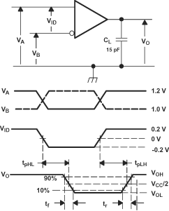
A. All input pulses are supplied by a
generator having the following characteristics: tr or tf ≤
1 ns, frequency = 1 MHz, duty cycle = 50 ± 5%. CL is a combination of
a 20%-tolerance, low-loss ceramic, surface-mount capacitor and fixture
capacitance within 2 cm of the D.U.T.
B. The measurement is made on test
equipment with a –3 dB bandwidth of at least 1 GHz.
Figure 7-10 Receiver
Timing Test Circuit and Waveforms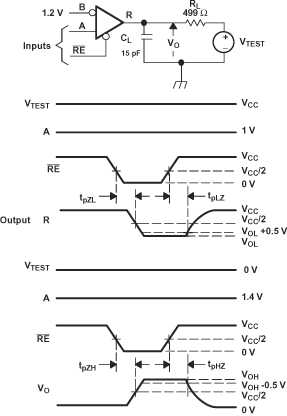
A. All input pulses are supplied by a
generator having the following characteristics: tr or tf ≤
1 ns, frequency = 1 MHz, duty cycle = 50 ± 5%.
B. RL is 1% tolerance, metal
film, surface mount, and located within 2 cm of the D.U.T.
C. CL is the instrumentation
and fixture capacitance within 2 cm of the DUT and ±20%.
Figure 7-11 Receiver
Enable and Disable Time Test Circuit and Waveforms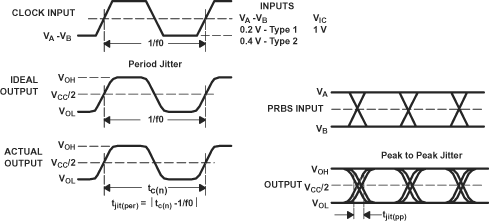
A. All input pulses are supplied by an
Agilent 8304A Stimulus System.
B. The measurement is made on a TEK
TDS6604 running TDSJIT3 application software
C. Period jitter is measured using a 50
MHz 50 ±1% duty cycle clock input.
D. Peak-to-peak jitter is measured
using a 100 Mbps 215 –1 PRBS input.
Figure 7-12 Receiver
Jitter Measurement Waveforms