SLLS755R July 2006 – October 2024 ISO7220A , ISO7220B , ISO7220C , ISO7220M , ISO7221A , ISO7221B , ISO7221C , ISO7221M
PRODUCTION DATA
- 1
- 1 Features
- 2 Applications
- 3 Description
- 4 Pin Configuration and Functions
-
5 Specifications
- 5.1 Absolute Maximum Ratings
- 5.2 ESD Ratings
- 5.3 Recommended Operating Conditions
- 5.4 Thermal Information
- 5.5 Power Ratings
- 5.6 Insulation Specifications
- 5.7 Safety-Related Certifications
- 5.8 Safety Limiting Values
- 5.9 Electrical Characteristics—5-V VCC1 and VCC2 Supplies
- 5.10 Electrical Characteristics—5-V VCC1 and 3.3-V VCC2 Supply
- 5.11 Electrical Characteristics—3.3-V VCC1 and 5-V VCC2 Supply
- 5.12 Electrical Characteristics—3.3-V VCC1 and VCC2 Supplies
- 5.13 Electrical Characteristics—2.8-V VCC1 and VCC2 Supplies
- 5.14 Switching Characteristics—5-V VCC1 and VCC2 Supplies
- 5.15 Switching Characteristics—5-V VCC1 and 3.3-V VCC2 Supply
- 5.16 Switching Characteristics—3.3-VCC1 and 5-V VCC2 Supplies
- 5.17 Switching Characteristics—3.3-V VCC1 and VCC2 Supplies
- 5.18 Switching Characteristics—2.8-V VCC1 and VCC2 Supplies
- 5.19 Insulation Characteristics Curves
- 5.20 Typical Characteristics
- 6 Parameter Measurement Information
- 7 Detailed Description
- 8 Application and Implementation
- 9 Device and Documentation Support
- 10Revision History
- 11Mechanical, Packaging, and Orderable Information
4 Pin Configuration and Functions
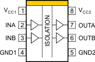
 Figure 4-1 ISO7220x D Package8-Pin SOICTop View
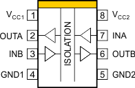
 Figure 4-2 ISO7221x D Package8-Pin SOICTop View
Table 4-1 Pin Functions
| PIN | Type(1) | DESCRIPTION | ||
|---|---|---|---|---|
| NAME | ISO7220x | ISO7221x | ||
| INA | 2 | 7 | I | Input, channel A |
| INB | 3 | 3 | I | Input, channel B |
| GND1 | 4 | 4 | — | Ground connection for VCC1 |
| GND2 | 5 | 5 | — | Ground connection for VCC2 |
| OUTA | 7 | 2 | O | Output, channel A |
| OUTB | 6 | 6 | O | Output, channel B |
| VCC1 | 1 | 1 | — | Power supply, VCC1 |
| VCC2 | 8 | 8 | — | Power supply, VCC2 |
(1) I = Input; O = Output