SLLS790E June 2007 – December 2024 TRS3232E
PRODUCTION DATA
- 1
- 1 Features
- 2 Applications
- 3 Description
- 4 Pin Configuration and Functions
-
5 Specifications
- 5.1 Absolute Maximum Ratings
- 5.2 ESD Ratings
- 5.3 ESD Ratings - IEC Specifications
- 5.4 Recommended Operating Conditions
- 5.5 Thermal Information
- 5.6 Electrical Characteristics — Device
- 5.7 Electrical Characteristics — Driver
- 5.8 Electrical Characteristics — Receiver
- 5.9 Switching Characteristics
- Typical Characteristics
- 6 Parameter Measurement Information
- 7 Detailed Description
- 8 Application and Implementation
- 9 Device and Documentation Support
- 10Revision History
- 11Mechanical, Packaging, and Orderable Information
3 Description
The TRS3232E device consists of two line drivers, two-line receivers, and a dual charge-pump circuit with ±15kV IEC ESD protection pin to pin (serial-port connection pins, including GND).
The device meets the requirements of TIA/EIA-232-F and provides the electrical interface between an asynchronous communication controller and the serial-port connector. The charge pump and four small external capacitors allow operation from a single 3V to 5.5V supply. The devices operate at data signaling rates up to 250kbps and a maximum of 30V/μs driver output slew rate.
| PART NUMBER | PACKAGE(1) | PACKAGE SIZE(2) |
|---|---|---|
| TRS3232E | SOIC (D, 16) | 9.9mm × 6mm |
| SSOP (DB, 16) | 6.2mm × 7.8mm | |
| SOIC (DW, 16) | 10.3mm × 10.3mm | |
| TSSOP (PW, 16) | 5mm × 6.4mm | |
| VQFN (RGT, 16) | 3mm x 3mm | |
| SOT-23-THN (DYY, 16) | 4.2mm × 2mm |
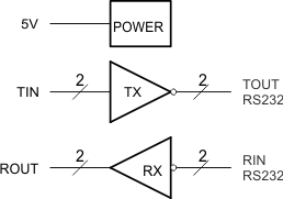
 Simplified Diagram