SLLS792C June 2007 – December 2024 TRS3221E
PRODUCTION DATA
- 1
- 1 Features
- 2 Applications
- 3 Description
- 4 Pin Configuration and Functions
-
5 Specifications
- 5.1 Absolute Maximum Ratings
- 5.2 ESD Ratings
- 5.3 ESD Ratings, IEC Specifications
- 5.4 Recommended Operating Conditions
- 5.5 Thermal Information
- 5.6 Electrical Characteristics
- 5.7 Driver Section Electrical Characteristics
- 5.8 Driver Section Switching Characteristics
- 5.9 Receiver Section Electrical Characteristics
- 5.10 Receiver Section Switching Characteristics
- 5.11 Auto-Powerdown Section Electrical Characteristics
- 5.12 Auto-Powerdown Section Switching Characteristics
- 5.13 Typical Characteristics
- 6 Parameter Measurement Information
- 7 Detailed Description
- 8 Application Information Disclaimer
- 9 Device and Documentation Support
- 10Revision History
- 11Mechanical, Packaging, and Orderable Information
5.13 Typical Characteristics
VCC = 3.3 V and TA = 25 °C unless specified otherwise.
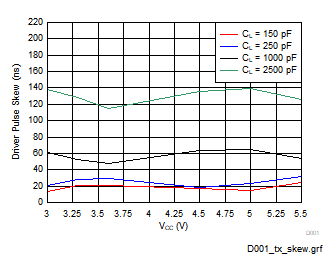
 Figure 5-1 Driver Pulse Skew vs Load Capacitance and Supply Voltage at TA =
25 °C (RGT Package)
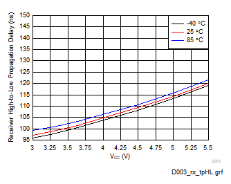
 Figure 5-3 Receiver Path High-to-Low
Propagation Delay vs TA and Supply Voltage (RGT Package).
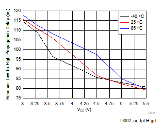
  Figure 5-2 Receiver Path Low-to-High Propagation Delay vs TA and Supply
Voltage (RGT Package)
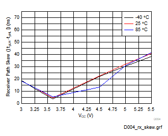
 Figure 5-4 Receiver Pulse Skew
(|tpLH - tpHL|) vs TA and Supply
Voltage (RGT Package).