SLLS902A February 2010 – March 2024 SN65MLVD040
PRODUCTION DATA
- 1
- 1 Features
- 2 Applications
- 3 Description
- 4 Pin Configuration and Functions
-
5 Specifications
- 5.1 Absolute Maximum Ratings
- 5.2 Reccommended Operationg Conditions
- 5.3 Thermal Characteristics
- 5.4 Package Dissipation Ratings
- 5.5 Device Electrical Characteristics
- 5.6 Driver Electrical Characteristics
- 5.7 Reciver Electrical Charecteristics
- 5.8 Bus Input and Output Electrical Characteristics
- 5.9 Driver Switching Characterisitics
- 5.10 Reciever Switching Charecteristics
- 5.11 Typical Characteristics
- 6 Paramater Measurement Information
- 7 Application and Implementation
- 8 Device and Documentation Support
- 9 Revision History
- 10Mechanical, Packaging, and Orderable Information
7.1.1 Source Synchronous System Clock (SSSC)
There are two approaches to transmit data in a synchronous system: centralized synchronous system clock (CSSC) and source synchronous system clock (SSSC). CSSC systems synchronize data transmission between different modules using a clock signal from a centralized source. The key requirement for a CSSC system is for data transmission and reception to complete during a single clock cycle. The maximum operating frequency is the inverse of the shortest clock cycle for which valid data transmission and reception can be ensured. SSSC systems achieve higher operating frequencies by sending clock and data signals together to eliminate the flight time on the transmission media, backplane, or cables. In SSSC systems, the maximum operating frequency is limited by the cumulated skews that can exist between clock and data. The absolute flight time of data on the backplane does not provide a limitation on the operating frequency as it does with CSSC.
The SN65MLVD082 can be designed for interfacing the data and clock to support source synchronous system clock (SSSC) operation. It is specified for transmitting data up to 250 Mbps and clock frequencies up to 125 MHz. Figure 7-1 shows an example of a SSSC architecture supported by M-LVDS transceivers. The SN65MLVD206, a single channel transceiver, transmits the main system clock between modules. A retiming unit is then applied to the main system clock to generate a local clock for subsystem synchronization processing. System operating data (or control) and subsystem clock signals are generated from the data processing unit, such as a microprocessor, FPGA, or ASIC, on module 1, and sent to slave modules through the SN65MLVD082. Such design configurations are common while transmitting parallel control data over the backplane with a higher SSSC subsystem clock frequency. The subsystem clock frequency is aligned with the operating frequencies of the data processing unit to synchronize data transmission between different units.
 Figure 7-1 Using
Differential M-LVDS to Perform Source Synchronous System Clock
Distribution
Figure 7-1 Using
Differential M-LVDS to Perform Source Synchronous System Clock
DistributionThe maximum SSSC frequencies in a transparent mode can be calculated with Equation 1:
Setup time and hold time on the receiver side are decided by the data processing unit, FPGA, or ASIC in this example. By considering data passes through the transceiver only, the general calculation result is 238 MHz when using the following data:
tsk(o)Source = 2 ns – Output skew of data processing unit; any skew between data bits, or clock and data bits
tsk(pp)DRVR = 0.6 ns – Driver part-to-part skew of the SN65MLVD040
tsk(flight)BP = 0.4 ns – Skew of propagation delay on the backplane between data and clock
tsk(pp)RCVR = 1 ns – Receiver part-to-part skew of the SN65MLVD040
The 238-MHz maximum operating speed calculated above was determined based on data and clock skews only. Another important consideration when calculating the maximum operating speed is output transition time. Transition-time-limited operating speed is calculated from Equation 2:
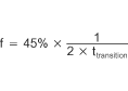
Using the typical transition time of the SN65MLVD040 of 1.4 ns, a transition-time-limited operating frequency of 170 MHz can be supported.
In addition to the high operating frequencies of SSSC that can be ensured, the SN65MLVD040 presents other benefits as other M-LVDS bus transceivers can provide:
- Robust system operation due to common mode noise cancellation using a low voltage differential receiver
- Low EMI radiation noise due to differential signaling improves signal integrity through the backplane
- A singly terminated transmission line is easy to design and implement
- Low power consumption in both active and idle modes minimizes thermal concerns on each module
In dense backplane design, these benefits are important for improving the performance of the whole system.