SLLS902A February 2010 – March 2024 SN65MLVD040
PRODUCTION DATA
- 1
- 1 Features
- 2 Applications
- 3 Description
- 4 Pin Configuration and Functions
-
5 Specifications
- 5.1 Absolute Maximum Ratings
- 5.2 Reccommended Operationg Conditions
- 5.3 Thermal Characteristics
- 5.4 Package Dissipation Ratings
- 5.5 Device Electrical Characteristics
- 5.6 Driver Electrical Characteristics
- 5.7 Reciver Electrical Charecteristics
- 5.8 Bus Input and Output Electrical Characteristics
- 5.9 Driver Switching Characterisitics
- 5.10 Reciever Switching Charecteristics
- 5.11 Typical Characteristics
- 6 Paramater Measurement Information
- 7 Application and Implementation
- 8 Device and Documentation Support
- 9 Revision History
- 10Mechanical, Packaging, and Orderable Information
5.11 Typical Characteristics
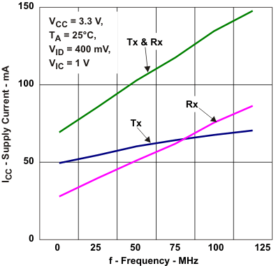 Figure 5-1 Supply Current vs
Frequency
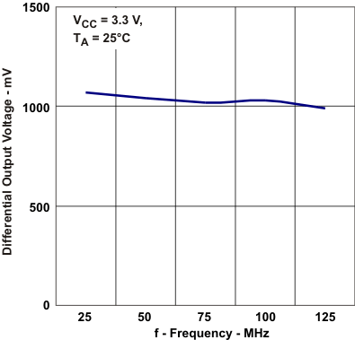 Figure 5-3 Differntial Output Voltage
vs Frequency
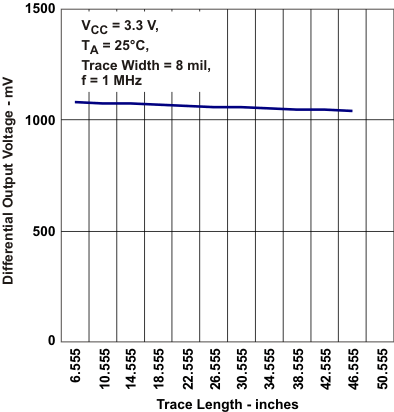 Figure 5-5 Differential Output
Voltage vs Trace Length
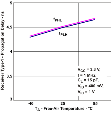 Figure 5-7 Receiver Type-1
Propagation Delay vs Free-air Temperature
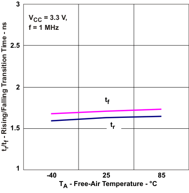 Figure 5-9 Driver Transition Time vs
Free-air Temperature
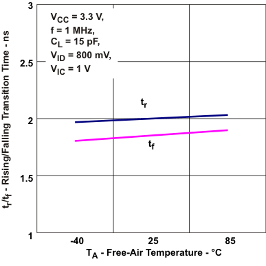 Figure 5-11 Type-2 Reciver Transition
Time vs Free-Air Temperature
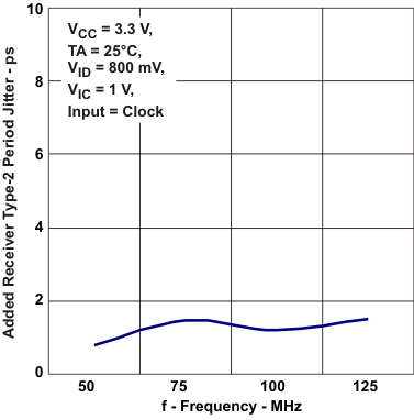 Figure 5-13 Added Reciver Type-2
Periods Jitter vs Frequency
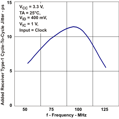 Figure 5-15 Added Reciver Type-1
Cycle-to-Cycle Jitter vs Frequency
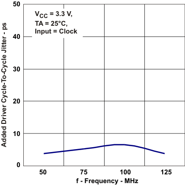 Figure 5-17 Added Driver
Cycle-to-Cylce Jitter vs Frequency
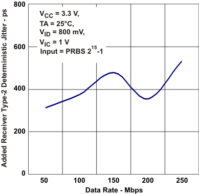 Figure 5-19 Added Reciver Type-1
Deterministic Jitter vs Data Rate
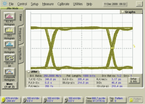 Figure 5-21 Reciver Output Eye Pattern
250 Mbps, 215–1 PRBS, VCC = 3.3 V|VID| =
400 mVPP, VIC = 1 V
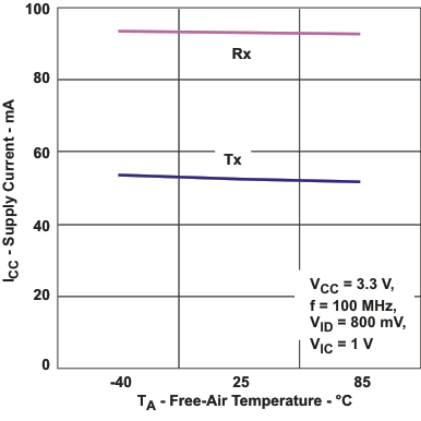 Figure 5-2 Supply Current vs Free-air
Temperature
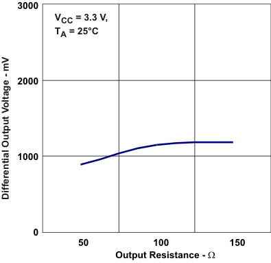 Figure 5-4 Differential Output
Voltage vs Frequency
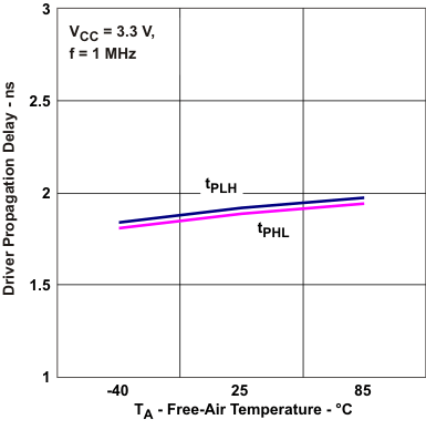 Figure 5-6 Driver Propagation Delay
vs Free-Air Temperature
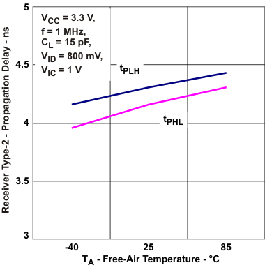 Figure 5-8 Receiver Type-2
Propagation Delay vs Free-air Temperature
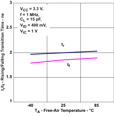 Figure 5-10 Type-1 Reciver Transition
Time vs Free-Air Temperature
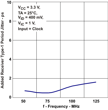 Figure 5-12 Added Reciver Type-1
Period Jitter vs Frequency
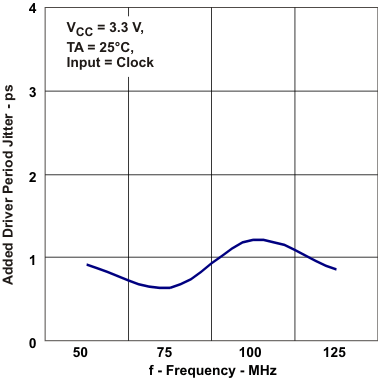 Figure 5-14 Added Period Driver Jitter
vs Frequency
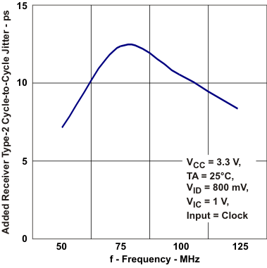 Figure 5-16 Added Reciver Type-2
Cycle-to-Cycle Jitter vs Frequency
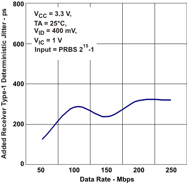 Figure 5-18 Added Reciver Type-1
Deterministic Jitter vs Data Rate
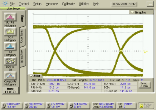 Figure 5-20 Driver Output Eye Pattern
250 Mbps, 215–1 PRBS, VCC = 3.3 V
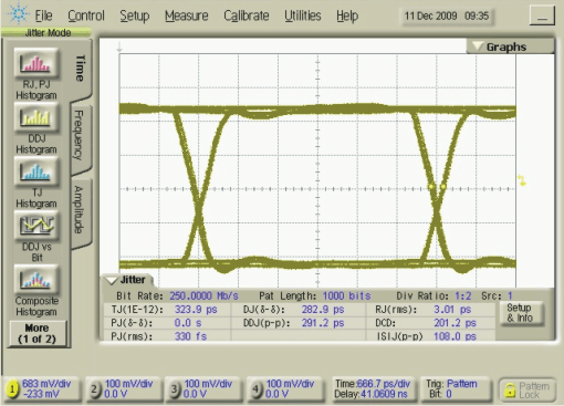 Figure 5-22 Reciver Output Eye Pattern
250 Mbps, 215–1 PRBS, VCC = 3.3 V|VID| =
800 mVPP, VIC = 1 V