SLLS902A February 2010 – March 2024 SN65MLVD040
PRODUCTION DATA
- 1
- 1 Features
- 2 Applications
- 3 Description
- 4 Pin Configuration and Functions
-
5 Specifications
- 5.1 Absolute Maximum Ratings
- 5.2 Reccommended Operationg Conditions
- 5.3 Thermal Characteristics
- 5.4 Package Dissipation Ratings
- 5.5 Device Electrical Characteristics
- 5.6 Driver Electrical Characteristics
- 5.7 Reciver Electrical Charecteristics
- 5.8 Bus Input and Output Electrical Characteristics
- 5.9 Driver Switching Characterisitics
- 5.10 Reciever Switching Charecteristics
- 5.11 Typical Characteristics
- 6 Paramater Measurement Information
- 7 Application and Implementation
- 8 Device and Documentation Support
- 9 Revision History
- 10Mechanical, Packaging, and Orderable Information
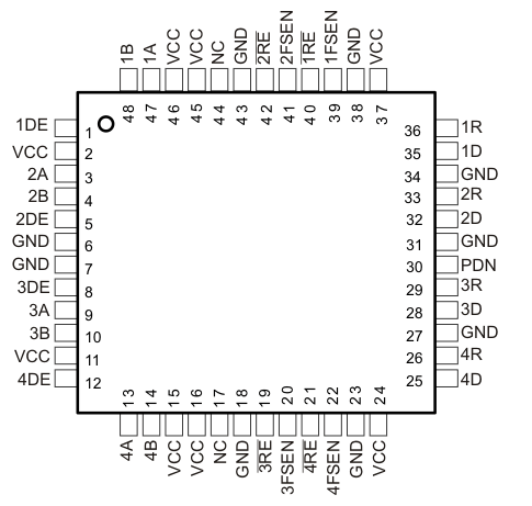
4 Pin Configuration and Functions
 Figure 4-1 RGZ Package(Top View)
Table 4-1 Pin Functions
| PIN | I/O | DESCRIPTION | |
|---|---|---|---|
| NAME | NO. | ||
| 1D–4D | 35, 32, 28, 25 | I | Data inputs for drivers |
| 1R–4R | 36, 33, 29, 26 | O | Data output for receivers |
| 1A–4A | 47, 3, 9, 13 | Bus I/O | M-LVDS bus non-inverting input/output |
| 1B–4B | 48, 4, 10, 14 | Bus I/O | M-LVDS bus inverting input/output |
| GND | 6, 7, 18, 23, 27, 31, 34, 38, 43 | Circuit ground. ALL GND pins must be connected to ground. | |
| VCC | 2, 11, 15, 16, 24, 37, 45, 46 | Supply voltage. ALL VCC pins must be connected to supply. | |
| 1RE– 4RE | 40, 42, 19, 21 | I | Receiver enable, active low, enable individual receivers. When this pin is left floating, internally this pin will be pulled to logic HIGH. |
| 1DE–4DE | 1, 5, 8, 12 | I | Driver enable, active high, individual enables the drivers. When this pin is left floating, internally this pin will be pulled to logic LOW. |
| 1FSEN–4FSEN | 39, 41, 20, 22 | I | Failsafe enable pin. When this pin is left floating, internally
this pin will be pulled to logic HIGH. This pin enables the Type 2 receiver for the respective channel. xFSEN = L → Type 1 receiver inputs xFSEN = H → Type 2 receiver inputs |
| PDN | 30 | I | Power Down pin. When this pin is left floating, internally this pin
will be pulled to logic LOW. When PDN is HIGH, the device is powered up. When PDN is LOW, the device overrides all other control and powers down. All outputs are Hi-Z. |
| NC | 17 | Not Connected | |
| NC | 44 | Not Connected. Internal TI Test pin. This pin must be left unconnected. | |
| PowerPAD™ | – | Connected to GND | |
Table 4-2 Device Function Tables
| RECEIVER | DRIVER | |||||||||
|---|---|---|---|---|---|---|---|---|---|---|
| INPUTS(1) | RECEIVER TYPE | OUTPUT(1) | INPUTS(1) | OUTPUTS(1) | ||||||
| VID = VA – VB | PDN | FSEN | RE | R | D | DE | A | B | ||
| VID > 35 mV | H | L | L | Type 1 | H | L | H | L | H | |
| –35 mV ≤ VID ≤ 35 mV | H | L | L | Type 1 | ? | H | H | H | L | |
| VID < 35 mV | H | L | L | Type 1 | L | OPEN | H | L | H | |
| X | OPEN | Z | Z | |||||||
| VID > 135 mV | H | H | L | Type 2 | H | X | L | Z | Z | |
| 65 mV ≤ VID ≤ 135 mV | H | H | L | Type 2 | ? | |||||
| VID < 65 mV | H | H | L | Type 2 | L | |||||
| Open Circuit | H | L | L | Type 1 | ? | |||||
| Open Circuit | H | H | L | Type 2 | L | |||||
| X | H | X | H | X | Z | |||||
| X | H | X | OPEN | X | Z | |||||
| X | L | X | X | X | Z | |||||
(1) H=high level, L=low level, Z=high impedance, X=Don’t care,
?=indeterminate