SLLS902A February 2010 – March 2024 SN65MLVD040
PRODUCTION DATA
- 1
- 1 Features
- 2 Applications
- 3 Description
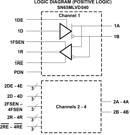
- 4 Pin Configuration and Functions
-
5 Specifications
- 5.1 Absolute Maximum Ratings
- 5.2 Reccommended Operationg Conditions
- 5.3 Thermal Characteristics
- 5.4 Package Dissipation Ratings
- 5.5 Device Electrical Characteristics
- 5.6 Driver Electrical Characteristics
- 5.7 Reciver Electrical Charecteristics
- 5.8 Bus Input and Output Electrical Characteristics
- 5.9 Driver Switching Characterisitics
- 5.10 Reciever Switching Charecteristics
- 5.11 Typical Characteristics
- 6 Paramater Measurement Information
- 7 Application and Implementation
- 8 Device and Documentation Support
- 9 Revision History
- 10Mechanical, Packaging, and Orderable Information
2 Applications
- Parallel Multipoint Data and Clock
Transmission Via Backplanes and Cables - Low-Power High-Speed Short-Reach Alternative to TIA/EIA-485
- Cellular Base Stations
- Central-Office Switches
- Network Switches and Routers
A. The signaling rate of a
line, is the number of voltage transitions that are made per second expressed in
the units bps (bits per second)