SLLSE11H March 2012 – March 2019 SN65HVD72 , SN65HVD75 , SN65HVD78
UNLESS OTHERWISE NOTED, this document contains PRODUCTION DATA.
- 1 Features
- 2 Applications
- 3 Description
- 4 Revision History
- 5 Device Comparison Table
- 6 Pin Configuration and Functions
-
7 Specifications
- 7.1 Absolute Maximum Ratings
- 7.2 ESD Ratings
- 7.3 Recommended Operating Conditions
- 7.4 Thermal Information
- 7.5 Electrical Characteristics
- 7.6 Power Dissipation
- 7.7 Switching Characteristics: 250 kbps Device (SN65HVD72) Bit Time ≥ 4 µs
- 7.8 Switching Characteristics: 20 Mbps Device (SN65HVD75) Bit Time ≥50 ns
- 7.9 Switching Characteristics: 50 Mbps Device (SN65HVD78) Bit Time ≥20 ns
- 7.10 Typical Characteristics
- 8 Parameter Measurement Information
- 9 Detailed Description
- 10Application and Implementation
- 11Power Supply Recommendations
- 12Layout
- 13Device and Documentation Support
- 14Mechanical, Packaging, and Orderable Information
10.2.1.4 Receiver Failsafe
The differential receiver is failsafe to invalid bus states caused by:
- Open bus conditions such as a disconnected connector
- Shorted bus conditions such as cable damage shorting the twisted-pair together, or
- Idle bus conditions that occur when no driver on the bus is actively driving
Receiver failsafe is accomplished by offsetting the receiver thresholds such that the input-indeterminate range does not include zero volts differential. To comply with the RS-422 and RS-485 standards, the receiver output must output a high when the differential input VID is more positive than 200 mV, and must output a low when VID is more negative than –200 mV. The receiver parameters which determine the failsafe performance are VIT+, VIT–, and VHYS (the separation between VIT+ and VIT–). As shown in Electrical Characteristics, differential signals more negative than –200 mV will always cause a low receiver output, and differential signals more positive than 200 mV will always cause a high receiver output.
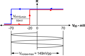
When the differential input signal is close to zero, it is still above the maximum VIT+ threshold of –20 mV, and the receiver output will be high. Only when the differential input is more than VHYS below VIT+ will the receiver output transition to a low state. Therefore, the noise immunity of the receiver inputs during a bus fault condition includes the receiver hysteresis value, VHYS, as well as the value of VIT+.
 Figure 22. SN65HVD7x Noise Immunity