SLLSE71A September 2011 – November 2024 ISO7231C-Q1
PRODUCTION DATA
- 1
- 1 Features
- 2 Applications
- 3 Description
-
4 Specifications
- 4.1 Absolute Maximum Ratings
- 4.2 ESD Ratings
- 4.3 Recommended Operating Conditions
- 4.4 Thermal Characteristics
- 4.5 Power Ratings
- 4.6 Insulation Specifications
- 4.7 Safety-Related Certifications
- 4.8 Safety Limiting Values
- 4.9 Electrical Characteristics: VCC1 and VCC2 at 3.3 V Operation
- 4.10 Electrical Characteristics: VCC1 and VCC2 at 5-V Operation
- 4.11 Electrical Characteristics: VCC1 at 3.3-V, VCC2 at 5-V Operation
- 4.12 Electrical Characteristics: VCC1 at 5-V, VCC2 at 3.3-V Operation
- 4.13 Switching Characteristics: VCC1 and VCC2 at 3.3-V Operation
- 4.14 Switching Characteristics: VCC1 and VCC2 at 5-V Operation
- 4.15 Switching Characteristics: VCC1 at 3.3-V and VCC2 at 5-V Operation
- 4.16 Switching Characteristics: VCC1 at 5-V, VCC2 at 3.3-V Operation
- 4.17 Typical Characteristics
- 5 Parameter Measurement Information
- 6 Detailed Description
- 7 Application and Implementation
- 8 Device and Documentation Support
- 9 Revision History
- 10Mechanical, Packaging, and Orderable Information
3 Description
The ISO7231C-Q1 are triple-channel digital isolators with multiple channel configurations and output enable functions. These devices have logic input and output buffers separated by TI’s silicon dioxide (SiO2) isolation barrier. Used in conjunction with isolated power supplies, these devices block high voltage, isolate grounds, and prevent noise currents on a data bus or other circuits from entering the local ground and interfering with or damaging sensitive circuitry.
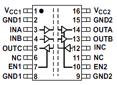
The ISO7231C-Q1 has two channels in one direction and one channel in opposition. These devices have an active-high output enable that when driven to a low level, places the output in a high-impedance state.
The ISO7231C-Q1 have TTL input thresholds and a noise-filter at the input that prevents transient pulses of up to 2ns in duration from being passed to the output of the device.
In each device, a periodic update pulse is sent across the isolation barrier to provide the proper dc level of the output. If this dc-refresh pulse is not received, the input is assumed to be unpowered or not being actively driven, and the failsafe circuit drives the output to a logic high state. (Contact TI for a logic low failsafe option).
These devices require two supply voltages of 3.3V, 5V, or any combination. All inputs are 5V tolerant when supplied from a 3.3V supply and all outputs are 4mA CMOS. These devices are characterized for operation over the ambient temperature range of –40°C to 125°C.
| DEVICE | PACKAGE(1) |
BODY SIZE (NOM) |
PACKAGE SIZE(2) |
|---|---|---|---|
| ISO7231C-Q1 | DW (SOIC, 16) |
10.30mm × 7.50mm |
10.30mm × 10.30mm |
 Figure 3-1 ISO7231C-Q1