SLLSEJ2G July 2015 – March 2020 SN65DP159 , SN75DP159
PRODUCTION DATA.
- 1 Features
- 2 Applications
- 3 Description
- 4 Revision History
- 5 Description (continued)
- 6 Pin Configuration and Functions
-
7 Specifications
- 7.1 Absolute Maximum Ratings
- 7.2 ESD Ratings
- 7.3 Recommended Operating Conditions
- 7.4 Thermal Information
- 7.5 Power Supply Electrical Characteristics
- 7.6 Differential Input Electrical Characteristics
- 7.7 HDMI and DVI TMDS Output Electrical Characteristics
- 7.8 AUX, DDC, and I2C Electrical Characteristics
- 7.9 HPD Electrical Characteristics
- 7.10 HDMI and DVI Main Link Switching Characteristics
- 7.11 AUX Switching Characteristics (Only for RGZ Package)
- 7.12 HPD Switching Characteristics
- 7.13 DDC and I2C Switching Characteristics
- 7.14 Typical Characteristics
- 8 Parameter Measurement Information
-
9 Detailed Description
- 9.1 Overview
- 9.2 Functional Block Diagram
- 9.3
Feature Description
- 9.3.1 Reset Implementation
- 9.3.2 Operation Timing
- 9.3.3 I2C-over-AUX to DDC Bridge (SNx5DP159 48-Pin Package Version Only)
- 9.3.4 Input Lane Swap and Polarity Working
- 9.3.5 Main Link Inputs
- 9.3.6 Main Link Inputs Debug Tools
- 9.3.7 Receiver Equalizer
- 9.3.8 Termination Impedance Control
- 9.3.9 TMDS Outputs
- 9.4 Device Functional Modes
- 9.5 Register Maps
- 10Application and Implementation
- 11Power Supply Recommendations
- 12Layout
- 13Device and Documentation Support
- 14Mechanical, Packaging, and Orderable Information
9.3.1 Reset Implementation
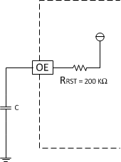
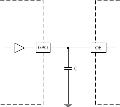
When OE is de-asserted, control signal inputs are ignored; the Dual Mode[1] DisplayPort inputs and outputs are high impedance. It is critical to transition the OE input from a low level to a high level after the VCC supply has reached the minimum recommended operating voltage. Achieve this transition by a control signal to the OE input, or by an external capacitor connected between OE and GND. To ensure that the SNx5DP159 device is properly reset, the OE pin must be de-asserted for at least 100-μs before being asserted. When OE is toggled in this manner the device is reset. This requires the device to be reprogrammed if it was originally programmed through I2C for configuration. When implementing the external capacitor, the size of the external capacitor depends on the power-up ramp of the VCC supply, where a slower ramp-up results in a larger value external capacitor. Refer to the latest reference schematic for SNx5DP159; consider approximately 200-nF capacitor as a reasonable first estimate for the size of the external capacitor. Both OE implementations are shown in Figure 20 and Figure 21.
SPACE
 Figure 20. External Capacitor Controlled OE
  Figure 21. OE Input from Active Controller