SLLSEJ2G July 2015 – March 2020 SN65DP159 , SN75DP159
PRODUCTION DATA.
- 1 Features
- 2 Applications
- 3 Description
- 4 Revision History
- 5 Description (continued)
- 6 Pin Configuration and Functions
-
7 Specifications
- 7.1 Absolute Maximum Ratings
- 7.2 ESD Ratings
- 7.3 Recommended Operating Conditions
- 7.4 Thermal Information
- 7.5 Power Supply Electrical Characteristics
- 7.6 Differential Input Electrical Characteristics
- 7.7 HDMI and DVI TMDS Output Electrical Characteristics
- 7.8 AUX, DDC, and I2C Electrical Characteristics
- 7.9 HPD Electrical Characteristics
- 7.10 HDMI and DVI Main Link Switching Characteristics
- 7.11 AUX Switching Characteristics (Only for RGZ Package)
- 7.12 HPD Switching Characteristics
- 7.13 DDC and I2C Switching Characteristics
- 7.14 Typical Characteristics
- 8 Parameter Measurement Information
-
9 Detailed Description
- 9.1 Overview
- 9.2 Functional Block Diagram
- 9.3
Feature Description
- 9.3.1 Reset Implementation
- 9.3.2 Operation Timing
- 9.3.3 I2C-over-AUX to DDC Bridge (SNx5DP159 48-Pin Package Version Only)
- 9.3.4 Input Lane Swap and Polarity Working
- 9.3.5 Main Link Inputs
- 9.3.6 Main Link Inputs Debug Tools
- 9.3.7 Receiver Equalizer
- 9.3.8 Termination Impedance Control
- 9.3.9 TMDS Outputs
- 9.4 Device Functional Modes
- 9.5 Register Maps
- 10Application and Implementation
- 11Power Supply Recommendations
- 12Layout
- 13Device and Documentation Support
- 14Mechanical, Packaging, and Orderable Information
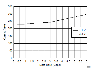
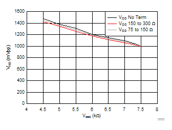
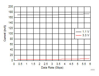
7.14 Typical Characteristics


