SLLSEJ4B July   2016  – June 2018 SN65DSI85-Q1

PRODUCTION DATA.  

  1. Features
  2. Applications
  3. Description
    1.     Typical Application
  4. Revision History
  5. Pin Configuration and Functions
    1.     Pin Functions
  6. Specifications
    1. 6.1 Absolute Maximum Ratings
    2. 6.2 ESD Ratings
    3. 6.3 Recommended Operating Conditions
    4. 6.4 Thermal Information
    5. 6.5 Electrical Characteristics
    6. 6.6 Switching Characteristics
  7. Parameter Measurement Information
  8. Detailed Description
    1. 8.1 Overview
    2. 8.2 Functional Block Diagram
    3. 8.3 Feature Description
      1. 8.3.1 Reset Implementation
      2. 8.3.2 Initialization Setup
      3. 8.3.3 LVDS Output Formats
      4. 8.3.4 DSI Lane Merging
      5. 8.3.5 DSI Pixel Stream Packets
      6. 8.3.6 DSI Video Transmission Specifications
      7. 8.3.7 ULPS
      8. 8.3.8 LVDS Pattern Generation
    4. 8.4 Device Functional Modes
      1. 8.4.1 Operating Modes
    5. 8.5 Programming
      1. 8.5.1 Clock Configurations and Multipliers
    6. 8.6 Register Maps
      1. 8.6.1 Local I2C Interface Overview
        1. 8.6.1.1 Write Procedure
        2. 8.6.1.2 Read Procedure
        3. 8.6.1.3 Setting a Starting Sub-Address Procedure
      2. 8.6.2 Control and Status Registers Overview
      3. 8.6.3 CSR Bit
        1. 8.6.3.1 ID Registers (address = 0x00 to 0x08)
          1. Table 7. ID Register Field Descriptions
        2. 8.6.3.2 Reset and Clock Registers
          1. 8.6.3.2.1 Address 0x09
            1. Table 8. Address 0x09 Definitions
          2. 8.6.3.2.2 Address 0x0A
            1. Table 9. Address 0x0A Field Descriptions
          3. 8.6.3.2.3 Address 0x0B
            1. Table 10. Address 0x0B Field Descriptions
          4. 8.6.3.2.4 Address 0x0D
            1. Table 11. Address 0x0D Field Descriptions
        3. 8.6.3.3 DSI Registers
          1. 8.6.3.3.1 Address 0x10
            1. Table 12. Address 0x10 Field Descriptions
          2. 8.6.3.3.2 Address 0x11
            1. Table 13. Address 0x11 Field Descriptions
          3. 8.6.3.3.3 Address 0x12
            1. Table 14. Address 0x12 Field Descriptions
          4. 8.6.3.3.4 Address 0x13
            1. Table 15. Address 0x13 Field Descriptions
        4. 8.6.3.4 LVDS Registers
          1. 8.6.3.4.1 Address 0x18
            1. Table 16. Address 0x18 Field Descriptions
          2. 8.6.3.4.2 Address 0x19
            1. Table 17. Address 0x19 Field Descriptions
          3. 8.6.3.4.3 Address 0x1A
            1. Table 18. Address 0x1A Field Descriptions
          4. 8.6.3.4.4 Address 0x1B
            1. Table 19. Address 0x1B Field Descriptions
        5. 8.6.3.5 Video Registers
          1. 8.6.3.5.1  Address 0x20
            1. Table 20. Address 0x20 Field Descriptions
          2. 8.6.3.5.2  Address 0x21
            1. Table 21. Address 0x21 Field Descriptions
          3. 8.6.3.5.3  Address 0x22
            1. Table 22. Address 0x22 Field Descriptions
          4. 8.6.3.5.4  Address 0x23
            1. Table 23. Address 0x23 Field Descriptions
          5. 8.6.3.5.5  Address 0x24
            1. Table 24. Address 0x24 Field Descriptions
          6. 8.6.3.5.6  Address 0x25
            1. Table 25. Address 0x25 Field Descriptions
          7. 8.6.3.5.7  Address 0x26
            1. Table 26. Address 0x26 Field Descriptions
          8. 8.6.3.5.8  Address 0x27
            1. Table 27. Address 0x27 Field Descriptions
          9. 8.6.3.5.9  Address 0x28
            1. Table 28. Address 0x28 Field Descriptions
          10. 8.6.3.5.10 Address 0x29
            1. Table 29. Address 0x29 Field Descriptions
          11. 8.6.3.5.11 Address 0x2A
            1. Table 30. Address 0x2A Field Descriptions
          12. 8.6.3.5.12 Address 0x2B
            1. Table 31. Address 0x2B Field Descriptions
          13. 8.6.3.5.13 Address 0x2C
            1. Table 32. Address 0x2C Field Descriptions
          14. 8.6.3.5.14 Address 0x2D
            1. Table 33. Address 0x2D Field Descriptions
          15. 8.6.3.5.15 Address 0x2E
            1. Table 34. Address 0x2E Field Descriptions
          16. 8.6.3.5.16 Address 0x2F
            1. Table 35. Address 0x2F Field Descriptions
          17. 8.6.3.5.17 Address 0x30
            1. Table 36. Address 0x30 Field Descriptions
          18. 8.6.3.5.18 Address 0x31
            1. Table 37. Address 0x31 Field Descriptions
          19. 8.6.3.5.19 Address 0x32
            1. Table 38. Address 0x32 Field Descriptions
          20. 8.6.3.5.20 Address 0x33
            1. Table 39. Address 0x33 Field Descriptions
          21. 8.6.3.5.21 Address 0x34
            1. Table 40. Address 0x34 Field Descriptions
          22. 8.6.3.5.22 Address 0x35
            1. Table 41. Address 0x35 Field Descriptions
          23. 8.6.3.5.23 Address 0x36
            1. Table 42. Address 0x36 Field Descriptions
          24. 8.6.3.5.24 Address 0x37
            1. Table 43. Address 0x37 Field Descriptions
          25. 8.6.3.5.25 Address 0x38
            1. Table 44. Address 0x38 Field Descriptions
          26. 8.6.3.5.26 Address 0x39
            1. Table 45. Address 0x39 Field Descriptions
          27. 8.6.3.5.27 Address 0x3A
            1. Table 46. Address 0x3A Field Descriptions
          28. 8.6.3.5.28 Address 0x3B
            1. Table 47. Address 0x3B Field Descriptions
          29. 8.6.3.5.29 Address 0x3C
            1. Table 48. Address 0x3C Field Descriptions
          30. 8.6.3.5.30 Address 0x3D
            1. Table 49. Address 0x3D Field Descriptions
          31. 8.6.3.5.31 Address 0x3E
            1. Table 50. Address 0x3E Field Descriptions
        6. 8.6.3.6 IRQ Registers
          1. 8.6.3.6.1 Address 0xE0
            1. Table 51. Address 0xE0 Field Descriptions
          2. 8.6.3.6.2 Address 0xE1
            1. Table 52. Address 0xE1 Field Descriptions
          3. 8.6.3.6.3 Address 0xE2
            1. Table 53. Address 0xE2 Field Descriptions
          4. 8.6.3.6.4 Address 0xE5
            1. Table 54. Address 0xE5 Field Descriptions
          5. 8.6.3.6.5 Address 0xE6
            1. Table 55. Address 0xE6 Field Descriptions
  9. Application and Implementation
    1. 9.1 Application Information
      1. 9.1.1 Video STOP and Restart Sequence
      2. 9.1.2 Reverse LVDS Pin Order Option
      3. 9.1.3 IRQ Usage
    2. 9.2 Typical Applications
      1. 9.2.1 Typical WUXGA 18-bpp Application
        1. 9.2.1.1 Design Requirements
        2. 9.2.1.2 Detailed Design Procedure
          1. 9.2.1.2.1 Example Script
        3. 9.2.1.3 Application Curve
      2. 9.2.2 Typical WQXGA 24-bpp Application
        1. 9.2.2.1 Design Requirements
  10. 10Power Supply Recommendations
    1. 10.1 VCC Power Supply
    2. 10.2 VCORE Power Supply
  11. 11Layout
    1. 11.1 Layout Guidelines
      1. 11.1.1 Package Specific
      2. 11.1.2 Differential pairs
      3. 11.1.3 Ground
    2. 11.2 Layout Example
  12. 12Device and Documentation Support
    1. 12.1 Documentation Support
      1. 12.1.1 Related Documentation
    2. 12.2 Receiving Notification of Documentation Updates
    3. 12.3 Community Resource
    4. 12.4 Trademarks
    5. 12.5 Electrostatic Discharge Caution
    6. 12.6 Glossary
  13. 13Mechanical, Packaging, and Orderable Information

DSI Video Transmission Specifications

The SN65DSI85-Q1 supports burst video mode and non-burst video mode with sync events or with sync pulses packet transmission as described in the DSI specification. The burst mode supports time-compressed pixel stream packets that leave added time per scan line for power savings LP mode. The SN65DSI85-Q1 requires a transition to LP mode once per frame to enable PHY synchronization with the DSI host processor; however, for a robust and low-power implementation, the transition to LP mode is recommended on every video line.

Figure 17 shows the DSI video transmission applied to SN65DSI85-Q1 applications. In all applications, the LVDS output rate must be less than or equal to the DSI input rate. The first line of a video frame shall start with a VSS packet, and all other lines start with VSE or HSS. The position of the synchronization packets in time is of utmost importance since this has a direct impact on the visual performance of the display panel; that is, these packets generate the HS and VS (horizontal and vertical sync) signals on the LVDS interface after the delay programmed into CHA_SYNC_DELAY_LOW/HIGH (CSR 0x28.7:0 and 0x29.3:0) and/or CHB_SYNC_DELAY_LOW/HIGH (CSR 0x2A.7:0 and 0x2B.3:0). When configured for dual DSI channels, the SN65DSI85-Q1 uses the VSS, VSE, and HSS packets from channel A to generate the HS and VS (horizontal and vertical sync) signals on the LVDS interface, and the VSS, VSE, and HSS packets from channel B are ignored.

As required in the DSI specification, the SN65DSI85-Q1 requires that pixel stream packets contain an integer number of pixels (i.e. end on a pixel boundary); it is recommended to transmit an entire scan line on one pixel stream packet. When a scan line is broken in to multiple packets, inter-packet latency shall be considered such that the video pipeline (ie. pixel queue or partial line buffer) does not run empty (i.e. under-run); during scan line processing, if the pixel queue runs empty, the SN65DSI85-Q1 transmits zero data (18’b0 or 24’b0) on the LVDS interface.

When configured for dual DSI channels, the SN65DSI85-Q1 supports ODD/EVEN configurations and LEFT/RIGHT configurations. In the ODD/EVEN configuration, the odd pixels for each scan line are received on channel A, and the even pixels are received on channel B. In LEFT/RIGHT mode, the LEFT portion of the line is received on channel A, and the right portion of the line is received on channel B. Neither the channel A LEFT portion input or the channel B RIGHT portion input per line shall exceed 1408 pixels, which is defined as ½ of the maximum line size (2560 pixels in WQXGA 2560x1600 mode) plus 10% headroom. The pixels received on channel B in LEFT/RIGHT mode are buffered during the LEFT side transmission to LVDS, and begin transmission to LVDS when the LEFT-side input buffer runs empty.

When configured for two single DSI channels, the SN65DSI85-Q1 requires that the LVDS output clocks for both video data streams be the same.

NOTE

When the HS clock is used as a source for the LVDS pixel clock, the LP mode transitions apply only to the data lanes, and the DSI clock lane remains in the HS mode during the entire video transmission.

The DSI85 does not support the DSI Virtual Channel capability or reverse direction (peripheral to processor) transmissions.
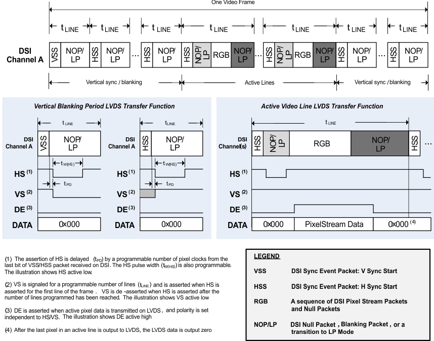
SN65DSI85-Q1 DSI_channel_tranmission_sllsej4.gifFigure 17. DSI Channel Transmission and Transfer Function