-
TMDS171/I 3.4 Gbps TMDS RETIMER
- 1 Features
- 2 Applications
- 3 Description
- 4 Revision History
- 5 Pin Configuration and Functions
- 6 Specifications
- 7 Parameter Measurement Information
-
8 Detailed Description
- 8.1 Overview
- 8.2 Functional Block Diagram
- 8.3
Feature Description
- 8.3.1 Reset Implementation
- 8.3.2 Operation Timing
- 8.3.3 Swap and Polarity Working (Retimer Mode Only)
- 8.3.4 TMDS Inputs
- 8.3.5 TMDS Inputs Debug Tools
- 8.3.6 Receiver Equalizer
- 8.3.7 Input Signal Detect Block
- 8.3.8 Audio Return Channel
- 8.3.9 Transmitter Impedance Control
- 8.3.10 TMDS Outputs
- 8.3.11 Pre-Emphasis/De-Emphasis
- 8.4 Device Functional Modes
- 8.5
Register Maps
- 8.5.1 Local I2C Overview
- 8.5.2 CSR Bit Field Definitions, DEVICE_ID (offset: 00000000 ≈ 00000111) (reset:00h ≈ 07h)
- 8.5.3 CSR Bit Field Definitions, REV _ID (offset: 00001000) (reset: 01h)
- 8.5.4 CSR BIT Field Definitions - Misc Control (offset: 00001001) (reset: 02h)
- 8.5.5 CSR BIT Field Definitions - Misc Control (offset: 00001010) (reset: B1h)
- 8.5.6 CSR BIT Field Definitions - Misc Control (offset: 00001011) (reset: 00h)
- 8.5.7 CSR BIT Field Definitions - Misc Control (offset: 00001100) (reset: 00h)
- 8.5.8 CSR BIT Field Definitions - Equalization Control Register (offset: 00001101) (reset: 01h)
- 8.5.9 CSR BIT Field Definitions - RX Pattern Verifier Control/Status (offset: 00001110) (reset: 00h)
- 8.5.10 CSR BIT Field Definitions - RX Pattern Verifier Control/Status (offset: 00001111) (reset: 00h)
- 8.5.11 CSR BIT Field Definitions - RX Pattern Verifier Control/Status (offset: 00010000) (reset: 00h)
- 8.5.12 CSR BIT Field Definitions - RX Pattern Verifier Control/Status (offset: 00010001) (reset: 00h)
- 8.5.13 CSR BIT Field Definitions - RX Pattern Verifier Control/Status (offset: 00010010) (reset: 00h)
- 8.5.14 CSR BIT Field Definitions - RX Pattern Verifier Control/Status (offset: 00010011) (reset: 00h)
- 8.5.15 CSR BIT Field Definitions - RX Pattern Verifier Control/Status (offset: 00010100) (reset: 00h)
- 8.5.16 CSR BIT Field Definitions - RX Pattern Verifier Control/Status (offset: 00010101) (reset: 00h)
- 8.5.17 CSR BIT Field Definitions - RX Pattern Verifier Control/Status (offset: 00010110) (reset: 00h)
- 8.5.18 CSR BIT Field Definitions - RX Pattern Verifier Control/Status (offset: 00010111) (reset: 00h)
- 8.5.19 CSR BIT Field Definitions - RX Pattern Verifier Control/Status (offset: 00011000) (reset: 00h)
- 8.5.20 CSR BIT Field Definitions - RX Pattern Verifier Control/Status (offset: 00011001) (reset: 00h)
- 8.5.21 CSR BIT Field Definitions - RX Pattern Verifier Control/Status (offset: 00011010) (reset: 00h)
- 8.5.22 CSR BIT Field Definitions - RX Pattern Verifier Control/Status (offset: 00011011) (reset: 00h)
- 8.5.23 CSR BIT Field Definitions - RX Pattern Verifier Control/Status (offset: 00011100) (reset: 00h)
- 8.5.24 CSR BIT Field Definitions - RX Pattern Verifier Control/Status (offset: 00011101) (reset: 00h)
- 8.5.25 CSR BIT Field Definitions - RX Pattern Verifier Control/Status (offset: 00011110) (reset: 00h)
- 8.5.26 CSR BIT Field Definitions - RX Pattern Verifier Control/Status (offset: 00011111) (reset: 00h)
- 8.5.27 CSR BIT Field Definitions - RX Pattern Verifier Control/Status (offset: 00100000) (reset: 00h)
- 9 Application and Implementation
- 10Power Supply Recommendations
- 11Layout
- 12Device and Documentation Support
- 13Mechanical, Packaging, and Orderable Information
- IMPORTANT NOTICE
TMDS171/I 3.4 Gbps TMDS RETIMER
1 Features
- HDMI Input Port to Output Port with CDR Supporting up to 3.4 Gbps Data Rates
- Compatible with HDMI1.4b Electrical Parameters.
- Support for 4k2k30p and up to WUXGA 12-bit Color Depth or 1080p with Higher Refresh Rates™
- Retimes Input Stream to Compensate for Random Jitter
- Adaptive Receiver Equalizer or Programmable Fixed Equalizer
- I2C and Pin Strap Programmable
- Inter-Pair Skew Compensation of 5+ Bits
- Link Debug Tools Including Eye Diagram After RX Equalizer
- Single Ended Mode ARC Support
- 48-pin 7mm x 7mm 0.5 mm Pitch VQFN Package
- Extended Commercial Temperature Support 0°C – 85°C (TMDS171)
- Industrial Temperature Support -40°C – 85°C (TMDS171I)
2 Applications
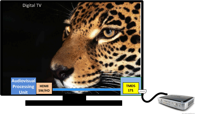
- Digital TV
- Digital Projector
- Audio/Video Equipment
- Blu-Ray DVD
- Monitors
- Desktops/ All-in-Ones
- Active Cables
3 Description
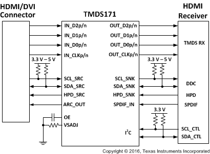
The TMDS171 is a digital video interface (DVI) or high-definition multimedia interface (HDMI) retimer. The TMDS171 supports four TMDS channels, Audio Return Channel (SPDIF_IN/ARC_OUT), Hot Plug Detect (HPD) and Digital Display Control (DDC) interfaces. The TMDS171 supports signaling rates up to 3.4 Gbps to allow for the highest resolutions of 4k2k30p 24 bits per pixel and up to WUXGA 12-bit color depth or 1080p with higher refresh rates. The TMDS171 automatically configures itself as a re-driver at low data rate (< 1 Gbps) or as a re-timer above this data rate.
The TMDS171 supports dual power supply rails of 1.2 V on VDD and 3.3 V on VCC for active power reduction. Several methods of power management are implemented to reduce overall power consumption. TMDS171 supports fixed EQ gain or adaptive EQ control by I2C or pin strap to compensate for different lengths input cable or board traces.
Device Information(1)
| PART NUMBER | PACKAGE | BODY SIZE (NOM) |
|---|---|---|
| TMDS171 | (VQFN) 48 Pins | 7.00 mm x 7.00 mm |
| TMDS171I |
- For all available packages, see the orderable addendum at the end of the data sheet.
Simplified Schematic |
 |
4 Revision History
Changes from D Revision (August 2016) to E Revision
- Added Note 3 to the Electrical Characteristics tableGo
- Deleted text "which is needed for certain HDMI CTS test." from the second paragraph in the Overview sectionGo
- Changed section: Input Signal Detect BlockGo
- Changed H to X in the first row of the HPD_SNK column in Table 36Go
- Changed the IN_Dx column in Table 36Go
Changes from C Revision (April 2016) to D Revision
- Recommended Operating Conditions, Changed the CONTROL PINS sectionGo
- Electrical Characteristics Changed the DDC and I2C sectionGo
Changes from B Revision (February 2016) to C Revision
- Changed pin 36 Description From: TX_TERM_CTL = L: 150 - 300 Ω To: TX_TERM_CTL = L: Reserved in the Pin Functions table Go
- Added OE to VIL "Low-level input voltage" in the Recommended Operating Conditions table Go
- Added OE to VIH "High-level input voltage" in the Recommended Operating Conditions table Go
- Changed Figure 23 Go
- Deleted the VDD_ramp and VCC_ramp MIN values in Table 1 Go
- Changed TX_TERM_CTL = L to Reserved in Table 3 Go
- Changed text "address 22h through the I2C interface" To: "address 0Bh through the I2C interface" DDC Functional DescriptionGo
- Added Note to 11–400-kbps in Table 8Go
- Added Note to 11–400-kbps in Table 10Go
Changes from A Revision (December 2015) to B Revision
- Changed Pin 44 From: AUX_SRCn To: ARC_OUT Pin 45 From: AUX_SRCn To: SPDIF_IN in the Pin Configuration and Functions image Go
Changes from * Revision (October 2015) to A Revision
- Changed the device status From: Product Preview To: Production Go