SLLSEQ1A September 2016 – December 2016 ISO5851-Q1
PRODUCTION DATA.
- 1 Features
- 2 Applications
- 3 Description
- 4 Revision History
- 5 Description (continued)
- 6 Pin Configuration and Function
-
7 Specifications
- 7.1 Absolute Maximum Ratings
- 7.2 ESD Ratings
- 7.3 Recommended Operating Conditions
- 7.4 Thermal Information
- 7.5 Power Ratings
- 7.6 Insulation Characteristics
- 7.7 Safety-Related Certifications
- 7.8 Safety Limiting Values
- 7.9 Electrical Characteristics
- 7.10 Switching Characteristics
- 7.11 Insulation Characteristics Curves
- 7.12 Typical Characteristics
- 8 Parameter Measurement Information
- 9 Detailed Description
-
10Application and Implementation
- 10.1 Application Information
- 10.2
Typical Applications
- 10.2.1 Design Requirements
- 10.2.2
Detailed Design Procedure
- 10.2.2.1 Recommended ISO5851-Q1 Application Circuit
- 10.2.2.2 FLT and RDY Pin Circuitry
- 10.2.2.3 Driving the Control Inputs
- 10.2.2.4 Local Shutdown and Reset
- 10.2.2.5 Global-Shutdown and Reset
- 10.2.2.6 Auto-Reset
- 10.2.2.7 DESAT Pin Protection
- 10.2.2.8 DESAT Diode and DESAT Threshold
- 10.2.2.9 Determining the Maximum Available, Dynamic Output Power, POD-max
- 10.2.2.10 Example
- 10.2.2.11 Higher Output Current Using an External Current Buffer
- 10.2.3 Application Curves
- 11Power Supply Recommendations
- 12Layout
- 13Device and Documentation Support
- 14Mechanical, Packaging, and Orderable Information
12 Layout
12.1 Layout Guidelines
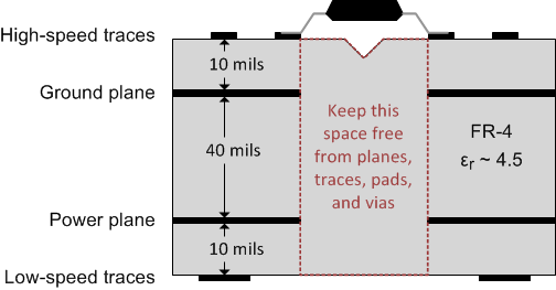
A minimum of four layers is required to accomplish a low EMI PCB design (see Figure 54). Layer stacking should be in the following order (top-to-bottom): high-current or sensitive signal layer, ground plane, power plane and low-frequency signal layer.
- Routing the high-current or sensitive traces on the top layer avoids the use of vias (and the introduction of their inductances) and allows for clean interconnects between the gate driver and the microcontroller and power transistors. Gate driver control input, Gate driver output OUT and DESAT should be routed in the top layer.
- Placing a solid ground plane next to the sensitive signal layer provides an excellent low-inductance path for the return current flow. On the driver side, use GND2 as the ground plane.
- Placing the power plane next to the ground plane creates additional high-frequency bypass capacitance of approximately 100 pF/inch2. On the gate-driver VEE2 and VCC2 can be used as power planes. They can share the same layer on the PCB as long as they are not connected together.
- Routing the slower speed control signals on the bottom layer allows for greater flexibility as these signal links usually have margin to tolerate discontinuities such as vias.
For detailed layout recommendations, see the Digital Isolator Design Guide (SLLA284).
12.2 PCB Material
For digital circuit boards operating at less than 150 Mbps, (or rise and fall times greater than 1 ns), and trace lengths of up to 10 inches, use standard FR-4 UL94V-0 printed circuit board. This PCB is preferred over cheaper alternatives because of lower dielectric losses at high frequencies, less moisture absorption, greater strength and stiffness, and the self-extinguishing flammability-characteristics.
12.3 Layout Example
 Figure 54. Recommended Layer Stack