SLLSEQ3A September 2016 – December 2016 ISO5451-Q1
PRODUCTION DATA.
- 1 Features
- 2 Applications
- 3 Description
- 4 Revision History
- 5 Description (continued)
- 6 Pin Configuration and Function
-
7 Specifications
- 7.1 Absolute Maximum Ratings
- 7.2 ESD Ratings
- 7.3 Recommended Operating Conditions
- 7.4 Thermal Information
- 7.5 Power Ratings
- 7.6 Insulation Characteristics
- 7.7 Safety-Related Certifications
- 7.8 Safety Limiting Values
- 7.9 Electrical Characteristics
- 7.10 Switching Characteristics
- 7.11 Insulation Characteristics Curves
- 7.12 Typical Characteristics
- 8 Parameter Measurement Information
- 9 Detailed Description
-
10Application and Implementation
- 10.1 Application Information
- 10.2
Typical Applications
- 10.2.1 Design Requirements
- 10.2.2
Detailed Design Procedure
- 10.2.2.1 Recommended ISO5451-Q1 Application Circuit
- 10.2.2.2 FLT and RDY Pin Circuitry
- 10.2.2.3 Driving the Control Inputs
- 10.2.2.4 Local Shutdown and Reset
- 10.2.2.5 Global-Shutdown and Reset
- 10.2.2.6 Auto-Reset
- 10.2.2.7 DESAT Pin Protection
- 10.2.2.8 DESAT Diode and DESAT Threshold
- 10.2.2.9 Determining the Maximum Available, Dynamic Output Power, POD-max
- 10.2.2.10 Example
- 10.2.2.11 Higher Output Current Using an External Current Buffer
- 10.2.3 Application Curves
- 11Power Supply Recommendations
- 12Layout
- 13Device and Documentation Support
- 14Mechanical, Packaging, and Orderable Information
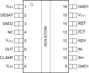
6 Pin Configuration and Function
DW Package
16-Pin SOIC
Top View

Pin Functions
| PIN | I/O | DESCRIPTION | |
|---|---|---|---|
| NAME | NO. | ||
| CLAMP | 7 | O | Miller clamp output |
| DESAT | 2 | I | Desaturation voltage input |
| FLT | 13 | O | Fault output, low-active during DESAT condition |
| GND1 | 9, 16 | — | Input ground |
| GND2 | 3 | — | Gate drive common. Connect to IGBT emitter |
| IN+ | 10 | I | Non-inverting gate drive voltage control input |
| IN– | 11 | I | Inverting gate drive voltage control input |
| NC | 4 | — | Not connected |
| OUT | 6 | O | Gate drive voltage output |
| RDY | 12 | O | Power-good output, active high when both supplies are good |
| RST | 14 | I | Reset input, apply a low pulse to reset fault latch |
| VCC1 | 15 | — | Positive input supply (3 V to 5.5 V) |
| VCC2 | 5 | — | Most positive output supply potential |
| VEE2 | 1, 8 | — | Output negative supply. Connect to GND2 for unipolar-supply application |