SLLSET5A March 2016 – September 2016 ISO7821LLS
PRODUCTION DATA.
- 1 Features
- 2 Applications
- 3 Description
- 4 Revision History
- 5 Pin Configuration and Functions
-
6 Specifications
- 6.1 Absolute Maximum Ratings
- 6.2 ESD Ratings
- 6.3 Recommended Operating Conditions
- 6.4 Thermal Information
- 6.5 Power Ratings
- 6.6 Insulation Specifications
- 6.7 Safety-Related Certifications
- 6.8 Safety Limiting Values
- 6.9 DC Electrical Characteristics
- 6.10 DC Supply Current Characteristics
- 6.11 Timing Requirements for Distortion Correction Scheme
- 6.12 Switching Characteristics
- 6.13 Insulation Characteristics Curves
- 6.14 Typical Characteristics
- 7 Parameter Measurement Information
- 8 Detailed Description
- 9 Application and Implementation
- 10Power Supply Recommendations
- 11Layout
- 12Device and Documentation Support
- 13Mechanical, Packaging, and Orderable Information
9 Application and Implementation
NOTE
Information in the following applications sections is not part of the TI component specification, and TI does not warrant its accuracy or completeness. TI’s customers are responsible for determining suitability of components for their purposes. Customers should validate and test their design implementation to confirm system functionality.
9.1 Application Information
The ISO7821LLS device is a high-performance, reinforced isolated dual-LVDS buffer. Isolation can be used to help achieve human and system safety, to overcome ground potential difference (GPD), or to improve noise immunity and system performance.
The LVDS signaling can be used over most interfaces to achieve higher data rates because the LVDS is only a physical layer. LVDS can also be used for a proprietary communication scheme implemented between a host controller and a slave. Example use cases include connecting a high-speed I/O module to a host controller, a subsystem connecting to a backplane, and connection between two high-speed subsystems. Many of these systems operate under harsh environments making them susceptible to electromagnetic interferences, voltage surges, electrical fast transients (EFT), and other disturbances. These systems must also meet strict limits on radiated emissions. Using isolation in combination with a robust low-noise signaling standard such as LVDS, achieves both high immunity to noise and low emissions.
Example end applications that could benefit from the ISO7821LLS device include high-voltage motor control, test and measurement, industrial automation, and medical equipment.
9.2 Typical Application
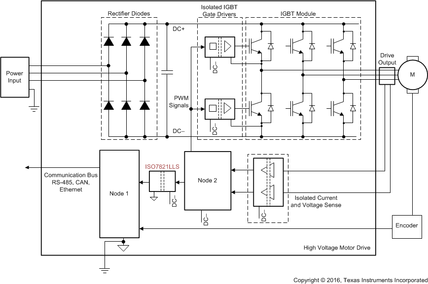
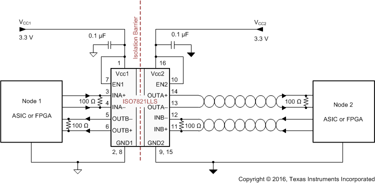
One application for isolated LVDS buffers is for point-to-point communication between two high-speed capable, application-specific integrated circuits (ASICs) or FPGAs. In a high-voltage motor control application, for example, Node 1 could be a controller on a low-voltage or earth referenced board, and Node 2, could be controller placed on the power board, biased to high voltage. Figure 27 and Figure 28 show the application schematics.
Figure 28 provides further details of using the ISO7821LLS device to isolate the LVDS interface. The LVDS connection to the ISO7821LLS device can be traces on a board (shown as straight lines between Node 1 and the ISO7821LLS device), a twisted pair cable (as shown between Node 2 and the ISO7821LLS device), or any other controlled impedance channel. Differential 100-Ω terminations are placed near each LVDS receiver. The characteristic impedance of the channel should also be 100-Ω differential.
In the example shown in Figure 27 and Figure 28, the ISO7821LLS device provides reinforced or safety isolation between the high-voltage elements of the motor drive and the low-voltage control circuitry. This configuration also ensures reliable communication, regardless of the high conducted and radiated noise present in the system.
 Figure 27. Isolated LVDS Interface in Motor Control Application
 Figure 28. Isolated LVDS Interface Between Two Nodes (ASIC or FPGA)
9.2.1 Design Requirements
For the ISO7821LLS device, use the parameters listed in Table 3.
Table 3. Design Parameters
| PARAMETER | VALUE |
|---|---|
| Supply voltage range, VCC1 and VCC2 | 3 V to 5.5 V |
| Receiver common-mode voltage range | 0.5 |VID| to 2.4 – 0.5 |VID| |
| External termination resistance | 100 Ω |
| Interconnect differential characteristic impedance | 100 Ω |
| Signaling rate | 50 to 150 Mbps |
| Decoupling capacitor from VCC1 and GND1 | 0.1 µF |
| Decoupling capacitor from VCC2 and GND2 | 0.1 µF |
9.2.2 Detailed Design Procedure
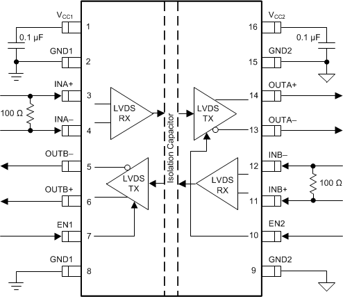
The ISO7821LLS device has minimum requirements on external components for correct operation. External bypass capacitors (0.1 µF) are required for both supplies (VCC1 and VCC2). A termination resistor with a value of 100 Ω is required between each differential input pair (INx+ and INx–), with the resistors placed as close to the device pins as possible. A differential termination resistor with a value of 100 Ω is required on the far end for the LVDS transmitters. Figure 29 shows these connections.
 Figure 29. Typical ISO7821LLS Circuit Hook-Up
9.2.2.1 Electromagnetic Compatibility (EMC) Considerations
Many applications in harsh industrial environment are sensitive to disturbances such as electrostatic discharge (ESD), electrical fast transient (EFT), surge and electromagnetic emissions. These electromagnetic disturbances are regulated by international standards such as IEC 61000-4-x and CISPR 22. Although system-level performance and reliability depends, to a large extent, on the application board design and layout, the ISO7821LLS device incorporates many chip-level design improvements for overall system robustness. Some of these improvements include:
- Robust ESD protection cells for input and output signal pins and inter-chip bond pads.
- Low-resistance connectivity of ESD cells to supply and ground pins.
- Enhanced performance of high voltage isolation capacitor for better tolerance of ESD, EFT and surge events.
- Bigger on-chip decoupling capacitors to bypass undesirable high energy signals through a low impedance path.
- PMOS and NMOS devices isolated from each other by using guard rings to avoid triggering of parasitic SCRs.
- Reduced common mode currents across the isolation barrier by ensuring purely differential internal operation.
9.2.3 Application Curve
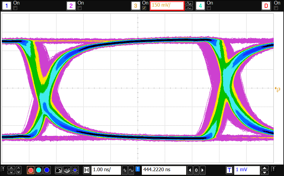
Figure 30 shows a typical eye diagram of the ISO7821LLS device which indicates low jitter and a wide-open eye at the maximum data rate of 150 Mbps.
 Figure 30. Eye Diagram at 150 Mbps PRBS, 3.3 V and 25°C