SLLSET5A March 2016 – September 2016 ISO7821LLS
PRODUCTION DATA.
- 1 Features
- 2 Applications
- 3 Description
- 4 Revision History
- 5 Pin Configuration and Functions
-
6 Specifications
- 6.1 Absolute Maximum Ratings
- 6.2 ESD Ratings
- 6.3 Recommended Operating Conditions
- 6.4 Thermal Information
- 6.5 Power Ratings
- 6.6 Insulation Specifications
- 6.7 Safety-Related Certifications
- 6.8 Safety Limiting Values
- 6.9 DC Electrical Characteristics
- 6.10 DC Supply Current Characteristics
- 6.11 Timing Requirements for Distortion Correction Scheme
- 6.12 Switching Characteristics
- 6.13 Insulation Characteristics Curves
- 6.14 Typical Characteristics
- 7 Parameter Measurement Information
- 8 Detailed Description
- 9 Application and Implementation
- 10Power Supply Recommendations
- 11Layout
- 12Device and Documentation Support
- 13Mechanical, Packaging, and Orderable Information
8 Detailed Description
8.1 Overview
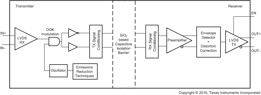
The ISO7821LLS device is an isolated LVDS buffer. The differential signal received on the LVDS input pins is first converted to CMOS logic levels. It is then transmitted across a silicon dioxide based capacitive isolation barrier using an On-Off Keying (OOK) modulation scheme. A high frequency carrier transmitted across the barrier represents one logic state and an absence of a carrier represents the other logic state. On the other side of the barrier a demodulator converts the OOK signal back to logic levels, which is then converted to LVDS outputs by a differential driver. This device incorporates advanced circuit techniques to maximize CMTI performance and minimize radiated emissions.
The ISO7821LLS device implements an eye-diagram improvement scheme to correct for signal distortions that are introduced in the LVDS receiver as well as the isolation channel. This enables the device to guarantee an eye closure of less than 30% at 125 Mbps, and less than 40% at 150 Mbps. The distortion correction scheme is optimized for operation with DC balanced data (for example 8b10b or equivalent) with a maximum run length of 6. The minimum data-rate of operation is also constrained to 50 Mbps. For general purpose data communication from 0 to 100 Mbps, the ISO782xLL family of devices should be considered.
The ISO7821LLS device is TIA/EIA-644-A standard compliant. The LVDS transmitter drives a minimum differential-output voltage magnitude of 250 mV into a 100-Ω load, and the LVDS receiver is capable of detecting differential signal ≥50 mV in magnitude. The device consumes 11 mA per channel at 150 Mbps with 5-V supplies.
The Functional Block Diagram section shows a conceptual block diagram of one channel of the ISO7821LLS device.
8.2 Functional Block Diagram

8.3 Feature Description
The ISO7821LLS device is available in a two-channel configuration with a default differential-high output state. Table 1 lists the device features.
Table 1. Device Features
| PART NUMBER | CHANNEL DIRECTION | RATED ISOLATION | MAXIMUM DATA RATE | DEFAULT DIFFERENTIAL OUTPUT |
|---|---|---|---|---|
| ISO7821LLS | 1 Forward, 1 Reverse | 5700 VRMS / 8000 VPK (1) | 150 Mbps | High |
8.3.1 Distortion-Correction Scheme
The ISO7821LLS device implements a distortion-correction scheme to correct for signal distortions that are introduced in the LVDS receiver as well as the isolation channel. This scheme is optimized for a DC-balanced data-stream with a maximum run length of 6. One example of such a data stream is 8b10b encoded data. The minimum data rate supported by the ISO7821LLS device is 50 Mbps and the maximum is 150 Mbps.
Figure 25 shows the timing requirements associated with the distortion correction scheme (see the Timing Requirements for Distortion Correction Scheme table for timing parameters). The input to the LVDS channel should be either idle low, idle high, or should have clock or DC-balanced data transitions at 25 MHz / 50 Mbps or higher. Low frequency or DC-unbalanced data is not allowed. The distortion-correction scheme runs an internal calibration each time the LVDS channel transitions from an idle state to a data transmission state. The calibration runs for a period of tCALIB during which the LVDS channel output is held at logic high. This calibration is also run at power up. Lack of activity on the receive inputs for a period greater than tIDLE_OUT takes the channel to an uncalibrated state. If the communication protocol requires the channel to transition to the idle state, the idle-high or idle-low state must be held for at least duration of tIDLE.

Logic high → VIN+ > VIN–
Logic low → VIN– > VIN+
Valid data = 8b10b like data with DC balance and bounded disparity.
8.4 Device Functional Modes
Table 2 lists the functional modes for the ISO7821LLS device.
Table 2. ISO7821LLS Function Table(1)
| VCCI | VCCO | INPUT (INx±)(2) |
OUTPUT ENABLE (ENx) |
OUTPUT (OUTx±)(3) |
COMMENTS |
|---|---|---|---|---|---|
| PU | PU | H | H or open | H | Normal Operation: A channel output assumes the logic state of the input. |
| L | H or open | L | |||
| I | H or open | H or L | |||
| X | PU | X | L | Z | A low-logic state at the output enable causes the outputs to be in high impedance. |
| PD | PU | X | H or open | H | Default mode: When VCCI is unpowered, a channel output assumes the logic high state. When VCCI transitions from unpowered to powered up, a channel output assumes the logic state of the input. When VCCI transitions from powered up to unpowered, a channel output assumes the selected default high state. |
| X | PD | X | X | Undetermined | When VCCO is unpowered, a channel output is undetermined. When VCCO transitions from unpowered to powered up, a channel output assumes the logic state of the input |
8.4.1 Device I/O Schematics
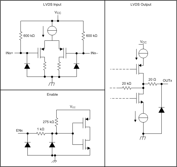
 Figure 26. Device I/O Schematics