SLLSEU7E November 2018 – July 2024 ISO7760-Q1 , ISO7761-Q1 , ISO7762-Q1 , ISO7763-Q1
PRODUCTION DATA
- 1
- 1 Features
- 2 Applications
- 3 Description
- 4 Description (Continued)
- 5 Pin Configuration and Functions
-
6 Specifications
- 6.1 Absolute Maximum Ratings
- 6.2 ESD Ratings
- 6.3 Recommended Operating Conditions
- 6.4 Thermal Information
- 6.5 Power Ratings
- 6.6 Insulation Specifications
- 6.7 Safety-Related Certifications
- 6.8 Safety Limiting Values
- 6.9 Electrical Characteristics—5-V Supply
- 6.10 Supply Current Characteristics—5-V Supply
- 6.11 Electrical Characteristics—3.3-V Supply
- 6.12 Supply Current Characteristics—3.3-V Supply
- 6.13 Electrical Characteristics—2.5-V Supply
- 6.14 Supply Current Characteristics—2.5-V Supply
- 6.15 Switching Characteristics—5-V Supply
- 6.16 Switching Characteristics—3.3-V Supply
- 6.17 Switching Characteristics—2.5-V Supply
- 6.18 Insulation Characteristics Curves
- 6.19 Typical Characteristics
- Parameter Measurement Information
- 7 Detailed Description
- 8 Application and Implementation
- 9 Power Supply Recommendations
- 10Layout
- 11Device and Documentation Support
- 12Revision History
- 13Mechanical, Packaging, and Orderable Information
3 Description
The ISO776x-Q1 devices are high-performance, six-channel digital isolators with 5000VRMS (DW package) and 3000VRMS (DBQ package) isolation ratings per UL 1577. This family of devices is also certified according to VDE, CSA, TUV and CQC.
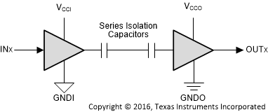
The ISO776x-Q1 family of devices provides high-electromagnetic immunity and low emissions at low-power consumption, while isolating CMOS or LVCMOS digital I/Os. Each isolation channel has a logic-input and logic-output buffer separated by a double capacitive silicon dioxide (SiO2) insulation barrier. The ISO776x-Q1 family of devices is available in all possible pin configurations such that all six channels are in the same direction, or one, two, or three channels are in reverse direction while the remaining channels are in forward direction. If the input power or signal is lost, the default output is high for devices without suffix F and low for devices with suffix F. See the Device Functional Modes section for further details.
| PART NUMBER | PACKAGE(1) | BODY SIZE (NOM) | PACKAGE SIZE(2) |
|---|---|---|---|
| ISO7760-Q1 ISO7761-Q1 ISO7762-Q1 IOS7763-Q1 |
SOIC (DW, 16) | 10.30mm × 7.50mm | 10.3mm × 10.30mm |
| SSOP (DBQ, 16) | 4.90mm × 3.90mm | 4.90mm × 6.00mm |
