SLLSEX2F December 2016 – April 2024 TDP158
PRODUCTION DATA
- 1
- 1 Features
- 2 Applications
- 3 Description
- 4 Pin Configuration and Functions
-
5 Specifications
- 5.1 Absolute Maximum Ratings
- 5.2 ESD Ratings
- 5.3 Recommended Operating Conditions
- 5.4 Thermal Information
- 5.5 Electrical Characteristics, Power Supply
- 5.6 Electrical Characteristics, Differential Input
- 5.7 Electrical Characteristics, TMDS Differential Output
- 5.8 Electrical Characteristics, DDC, I2C, HPD, and ARC
- 5.9 Electrical Characteristics, TMDS Differential Output in DP-Mode
- 5.10 Switching Characteristics, TMDS
- 5.11 Switching Characteristics, HPD
- 5.12 Switching Characteristics, DDC and I2C
- 5.13 Typical Characteristics
- 6 Parameter Measurement Information
-
7 Detailed Description
- 7.1 Overview
- 7.2 Functional Block Diagram
- 7.3 Feature Description
- 7.4 Device Functional Modes
- 7.5
Register Maps
- 7.5.1 Local I2C Control BIT Access TAG Convention
- 7.5.2 BIT Access Tag Conventions
- 7.5.3 CSR Bit Field Definitions, DEVICE_ID (address = 00h≅07h)
- 7.5.4 CSR Bit Field Definitions, REV_ID (address = 08h )
- 7.5.5 CSR Bit Field Definitions – MISC CONTROL 09h (address = 09h)
- 7.5.6 CSR Bit Field Definitions – MISC CONTROL 0Ah (address = 0Ah)
- 7.5.7 CSR Bit Field Definitions – MISC CONTROL 0Bh (address = 0Bh)
- 7.5.8 CSR Bit Field Definitions – MISC CONTROL 0Ch (address = 0Ch)
- 7.5.9 CSR Bit Field Definitions, Equalization Control Register (address = 0Dh)
- 7.5.10 CSR Bit Field Definitions, POWER MODE STATUS (address = 20h)
- 7.5.11 CSR Bit Field Definitions, DP-Mode and INDIVIDUAL LANE CONTROL (address = 30h)
- 7.5.12 CSR Bit Field Definitions, DP-Mode and INDIVIDUAL LANE CONTROL (address = 31h)
- 7.5.13 CSR Bit Field Definitions, DP-Mode and INDIVIDUAL LANE CONTROL (address = 32h)
- 7.5.14 CSR Bit Field Definitions, DP-Mode and INDIVIDUAL LANE CONTROL (address = 33h)
- 7.5.15 CSR Bit Field Definitions, DP-Mode and INDIVIDUAL LANE CONTROL (address = 34h)
- 7.5.16 CSR Bit Field Definitions, DP-Mode and INDIVIDUAL LANE CONTROL (address = 35h)
- 7.5.17 CSR Bit Field Definitions, DP-Mode and INDIVIDUAL LANE CONTROL (address = 4Dh)
- 7.5.18 CSR Bit Field Definitions, DP-Mode and INDIVIDUAL LANE CONTROL (address = 4Eh)
- 7.5.19 CSR Bit Field Definitions, DP-Mode and INDIVIDUAL LANE CONTROL (address = 4Fh)
- 8 Application and Implementation
- 9 Device and Documentation Support
- 10Revision History
- 11Mechanical, Packaging, and Orderable Information
7.3.9 TMDS Outputs
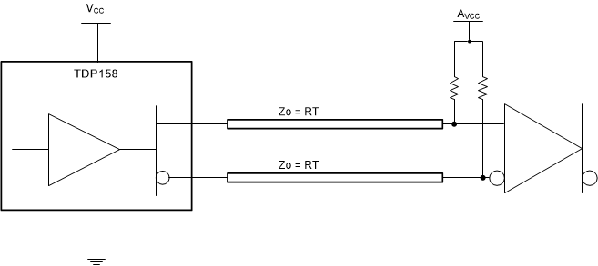
A 1% precision resistor, connected from VSADJ pin to ground is recommended to allow the differential output swing to comply with TMDS signal levels. The differential output driver provides a typical 10-mA current sink capability, which provides a typical 500mV voltage drop across a 50Ω termination resistor.
 Figure 7-5 TMDS Driver and Termination Circuit
Referring to Figure 7-5, if VCC (TDP158 supply) and AVCC (sink termination supply) are both powered, the TMDS output signals are high impedance when OE = low. Both supplies being active is the normal operating condition. A total of approximately 33-mW of power is consumed by the terminations independent of the OE logical selection. When AVCC is powered on, normal operation (OE controls output impedance) is resumed. When the power source of the device is off and the power source to termination is on, the IO(off), output leakage current, specification ensures the leakage current is limited 45-μA or less. The clock and data lanes VOD can be changed through I2C reg0Ch[7:2], VSWING_DATA and VSWING_CLK.