SLLSEX2F December 2016 – April 2024 TDP158
PRODUCTION DATA
- 1
- 1 Features
- 2 Applications
- 3 Description
- 4 Pin Configuration and Functions
-
5 Specifications
- 5.1 Absolute Maximum Ratings
- 5.2 ESD Ratings
- 5.3 Recommended Operating Conditions
- 5.4 Thermal Information
- 5.5 Electrical Characteristics, Power Supply
- 5.6 Electrical Characteristics, Differential Input
- 5.7 Electrical Characteristics, TMDS Differential Output
- 5.8 Electrical Characteristics, DDC, I2C, HPD, and ARC
- 5.9 Electrical Characteristics, TMDS Differential Output in DP-Mode
- 5.10 Switching Characteristics, TMDS
- 5.11 Switching Characteristics, HPD
- 5.12 Switching Characteristics, DDC and I2C
- 5.13 Typical Characteristics
- 6 Parameter Measurement Information
-
7 Detailed Description
- 7.1 Overview
- 7.2 Functional Block Diagram
- 7.3 Feature Description
- 7.4 Device Functional Modes
- 7.5
Register Maps
- 7.5.1 Local I2C Control BIT Access TAG Convention
- 7.5.2 BIT Access Tag Conventions
- 7.5.3 CSR Bit Field Definitions, DEVICE_ID (address = 00h≅07h)
- 7.5.4 CSR Bit Field Definitions, REV_ID (address = 08h )
- 7.5.5 CSR Bit Field Definitions – MISC CONTROL 09h (address = 09h)
- 7.5.6 CSR Bit Field Definitions – MISC CONTROL 0Ah (address = 0Ah)
- 7.5.7 CSR Bit Field Definitions – MISC CONTROL 0Bh (address = 0Bh)
- 7.5.8 CSR Bit Field Definitions – MISC CONTROL 0Ch (address = 0Ch)
- 7.5.9 CSR Bit Field Definitions, Equalization Control Register (address = 0Dh)
- 7.5.10 CSR Bit Field Definitions, POWER MODE STATUS (address = 20h)
- 7.5.11 CSR Bit Field Definitions, DP-Mode and INDIVIDUAL LANE CONTROL (address = 30h)
- 7.5.12 CSR Bit Field Definitions, DP-Mode and INDIVIDUAL LANE CONTROL (address = 31h)
- 7.5.13 CSR Bit Field Definitions, DP-Mode and INDIVIDUAL LANE CONTROL (address = 32h)
- 7.5.14 CSR Bit Field Definitions, DP-Mode and INDIVIDUAL LANE CONTROL (address = 33h)
- 7.5.15 CSR Bit Field Definitions, DP-Mode and INDIVIDUAL LANE CONTROL (address = 34h)
- 7.5.16 CSR Bit Field Definitions, DP-Mode and INDIVIDUAL LANE CONTROL (address = 35h)
- 7.5.17 CSR Bit Field Definitions, DP-Mode and INDIVIDUAL LANE CONTROL (address = 4Dh)
- 7.5.18 CSR Bit Field Definitions, DP-Mode and INDIVIDUAL LANE CONTROL (address = 4Eh)
- 7.5.19 CSR Bit Field Definitions, DP-Mode and INDIVIDUAL LANE CONTROL (address = 4Fh)
- 8 Application and Implementation
- 9 Device and Documentation Support
- 10Revision History
- 11Mechanical, Packaging, and Orderable Information
7.3.1 Reset Implementation
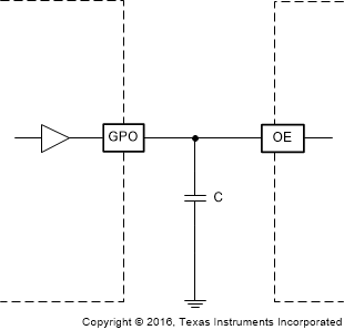
When OE is low, control signal inputs are ignored; the HDMI inputs and outputs are high impedance. It is critical to transition the OE from a low level to high after the VCC supply has reached the minimum recommended operating voltage. This is achieved by a control signal to the OE input, or by an external capacitor connected between OE and GND. To properly reset the TDP158, the OE pin must be de-asserted for at least 100 μs before being asserted. When OE is re-asserted the TDP158 must be reprogrammed if it was programmed by I2C and not pin strapping. When implementing the external capacitor, the size of the external capacitor depends on the power up ramp of the VCC supply, where a slower ramp-up results in a larger value external capacitor. Refer to the latest reference schematic for TDP158; consider approximately 0.1 µF capacitor as a reasonable first estimate for the size of the external capacitor. Both OE implementations are shown in Figure 7-1 and Figure 7-2.
 Figure 7-1 External Capacitor Controlled
OE
 Figure 7-2 OE Input from Active Controller