SLLSEX4B August   2019  – June 2022 TLIN1028-Q1

PRODUCTION DATA  

  1. Features
  2. Applications
  3. Description
  4. Revision History
  5. Description (continued)
  6. Pin Configuration and Functions
  7. Specifications
    1. 7.1 Absolute Maximum Ratings
    2. 7.2 ESD Ratings
    3. 7.3 ESD Ratings, IEC Specification
    4. 7.4 Recommended Operating Conditions
    5. 7.5 Thermal Information
    6. 7.6 Power Supply Characteristics
    7. 7.7 Electrical Charateristics
    8. 7.8 AC Switching Characteristics
    9. 7.9 Typical Characteristics
  8. Parameter Measurement Information
    1. 8.1 Test Circuit: Diagrams and Waveforms
  9. Detailed Description
    1. 9.1 Overview
    2. 9.2 Functional Block Diagram
    3. 9.3 Feature Description
      1. 9.3.1 LIN Pin
        1. 9.3.1.1 LIN Transmitter Characteristics
        2. 9.3.1.2 LIN Receiver Characteristics
          1. 9.3.1.2.1 Termination
      2. 9.3.2 TXD (Transmit Input)
      3. 9.3.3 RXD (Receive Output)
      4. 9.3.4 VSUP (Supply Voltage)
      5. 9.3.5 GND (Ground)
      6. 9.3.6 EN (Enable Input)
      7. 9.3.7 nRST (Reset Output)
      8. 9.3.8 VCC (Supply Output)
      9. 9.3.9 Protection Features
        1. 9.3.9.1 TXD Dominant Time Out (DTO)
        2. 9.3.9.2 Bus Stuck Dominant System Fault: False Wake Up Lockout
        3. 9.3.9.3 Thermal Shutdown
        4. 9.3.9.4 Under Voltage on VSUP
        5. 9.3.9.5 Unpowered Device and LIN Bus
    4. 9.4 Device Functional Modes
      1. 9.4.1 Normal Mode
      2. 9.4.2 Sleep Mode
      3. 9.4.3 Standby Mode
      4. 9.4.4 Wake-Up Events
        1. 9.4.4.1 Wake-Up Request (RXD)
      5. 9.4.5 Mode Transitions
      6. 9.4.6 Voltage Regulator
        1. 9.4.6.1 VCC
        2. 9.4.6.2 Output Capacitance Selection
        3. 9.4.6.3 Low-Voltage Tracking
        4. 9.4.6.4 Power Supply Recommendation
  10. 10Application and Implementation
    1. 10.1 Application Information
    2. 10.2 Typical Application
      1. 10.2.1 Design Requirements
        1. 10.2.1.1 Normal Mode Application Note
        2. 10.2.1.2 TXD Dominant State Timeout Application Note
        3. 10.2.1.3 Brownout
      2. 10.2.2 Detailed Design Procedures
      3. 10.2.3 Application Curves
  11. 11Power Supply Recommendations
  12. 12Layout
    1. 12.1 Layout Guidelines
    2. 12.2 Layout Example
  13. 13Device and Documentation Support
    1. 13.1 Documentation Support
      1. 13.1.1 Related Documentation
    2. 13.2 Related Links
    3. 13.3 Receiving Notification of Documentation Updates
    4. 13.4 Support Resources
    5. 13.5 Trademarks
    6. 13.6 Electrostatic Discharge Caution
    7. 13.7 Glossary
  14. 14Mechanical, Packaging, and Orderable Information
Termination

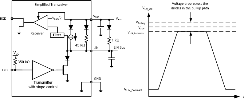
There is an internal pull-up resistor with a serial diode structure to VSUP, so no external pull-up components are required for the LIN responder node applications. An external pull-up resistor (1 kΩ) and a series diode to VSUP must be added when the device is used for commander node applications as per the LIN specification.

Figure 9-2 shows a commander node configuration and how the voltage levels are defined
GUID-8F5E2631-D1A4-41E3-90EB-AAB263AC0853-low.gifFigure 9-2 Commander Node Configuration with Voltage Levels