SLLSEZ5D January 2018 – June 2022 TCAN4550-Q1
PRODUCTION DATA
- 1 Features
- 2 Applications
- 3 Description
- 4 Revision History
- 5 Pin Configuration and Functions
-
6 Specification
- 6.1 Absolute Maximum Ratings
- 6.2 ESD Ratings
- 6.3 ESD Ratings, IEC ESD and ISO Transient Specification
- 6.4 Recommended Operating Conditions
- 6.5 Thermal Information
- 6.6 Supply Characteristics
- 6.7 Electrical Characteristics
- 6.8 Timing Requirements
- 6.9 Switching Characteristics
- 6.10 Typical Characteristics
- 7 Parameter Measurement Information
-
8 Detailed Description
- 8.1 Overview
- 8.2 Functional Block Diagram
- 8.3 Feature Description
- 8.4
Device Functional Modes
- 8.4.1 Normal Mode
- 8.4.2 Standby Mode
- 8.4.3 Sleep Mode
- 8.4.4 Test Mode
- 8.4.5 Failsafe Feature
- 8.4.6 Protection Features
- 8.4.7 CAN FD
- 8.5 Programming
- 8.6
Register Maps
- 8.6.1
Device ID and Interrupt/Diagnostic Flag Registers: 16'h0000 to 16'h002F
- 8.6.1.1 DEVICE_ID1[31:0] (address = h0000) [reset = h4E414354]
- 8.6.1.2 DEVICE_ID2[31:0] (address = h0004) [reset = h30353534]
- 8.6.1.3 Revision (address = h0008) [reset = h00110201]
- 8.6.1.4 Status (address = h000C) [reset = h0000000U]
- 8.6.1.5 SPI Error status mask (address = h0010) [reset = h00000000]
- 8.6.2 Device Configuration Registers: 16'h0800 to 16'h08FF
- 8.6.3 Interrupt/Diagnostic Flag and Enable Flag Registers: 16'h0820/0824 and 16'h0830
- 8.6.4
CAN FD Register Set: 16'h1000 to 16'h10FF
- 8.6.4.1 Core Release Register (address = h1000) [reset = hrrrddddd]
- 8.6.4.2 Endian Register (address = h1004) [reset = h87654321]
- 8.6.4.3 Customer Register (address = h1008) [reset = h00000000]
- 8.6.4.4 Data Bit Timing & Prescaler (address = h100C) [reset = h0000A33]
- 8.6.4.5 Test Register (address = h1010 ) [reset = h00000000]
- 8.6.4.6 RAM Watchdog (address = h1014) [reset = h00000000]
- 8.6.4.7 Control Register (address = h1018) [reset = 0000 0019]
- 8.6.4.8 Nominal Bit Timing & Prescaler Register (address = h101C) [reset = h06000A03]
- 8.6.4.9 Timestamp Counter Configuration (address = h1020) [reset = h00000000]
- 8.6.4.10 Timestamp Counter Value (address = h1024) [reset = h00000000]
- 8.6.4.11 Timeout Counter Configuration (address = h1028) [reset = hFFFF0000]
- 8.6.4.12 Timeout Counter Value (address = h102C) [reset = h0000FFFF]
- 8.6.4.13 Reserved (address = h1030 - h103C) [reset = h00000000]
- 8.6.4.14 Error Counter Register (address = h1040) [reset = h00000000]
- 8.6.4.15 Protocol Status Register (address = h1044) [reset = h00000707]
- 8.6.4.16 Transmitter Delay Compensation Register (address = h1048) [reset = h00000000]
- 8.6.4.17 Reserved (address = h104C) [reset = h00000000]
- 8.6.4.18 Interrupt Register (address = h1050) [reset = h00000000]
- 8.6.4.19 Interrupt Enable (address = h1054) [reset = h00000000]
- 8.6.4.20 Interrupt Line Select (address = h1058) [reset = h00000000]
- 8.6.4.21 Interrupt Line Enable (address = h105C) [reset = h00000000]
- 8.6.4.22 Reserved (address = h1060 - h107C) [reset = h00000000]
- 8.6.4.23 Global Filter Configuration (address = h1080) [reset = h00000000]
- 8.6.4.24 Standard ID Filter Configuration (address = h1084) [reset = h00000000]
- 8.6.4.25 Extended ID Filter Configuration (address = h1088) [reset = h00000000]
- 8.6.4.26 Reserved (address = h108C) [reset = h00000000]
- 8.6.4.27 Extended ID AND Mask (address = h1090) [reset = h1FFFFFFF]
- 8.6.4.28 High Priority Message Status (address = h1094) [reset = h00000000]
- 8.6.4.29 New Data 1 (address = h1098) [reset = h00000000]
- 8.6.4.30 New Data 2 (address = h109C) [reset = h00000000]
- 8.6.4.31 Rx FIFO 0 Configuration (address = h10A0) [reset = h00000000]
- 8.6.4.32 Rx FIFO 0 Status (address = h10A4) [reset = h00000000]
- 8.6.4.33 Rx FIFO 0 Acknowledge (address = h10A8) [reset = h00000000]
- 8.6.4.34 Rx Buffer Configuration (address = h10AC) [reset = h00000000]
- 8.6.4.35 Rx FIFO 1 Configuration (address = h10B0) [reset = h00000000]
- 8.6.4.36 Rx FIFO 1 Status (address = h10B4) [reset = h00000000]
- 8.6.4.37 Rx FIFO 1 Acknowledge (address = h10B8) [reset = h00000000]
- 8.6.4.38 Rx Buffer/FIFO Element Size Configuration (address = h10BC) [reset = h00000000]
- 8.6.4.39 Tx Buffer Configuration (address = h10C0) [reset = h00000000]
- 8.6.4.40 Tx FIFO/Queue Status (address = h10C4) [reset = h00000000]
- 8.6.4.41 Tx Buffer Element Size Configuration (address = h10C8) [reset = h00000000]
- 8.6.4.42 Tx Buffer Request Pending (address = h10CC) [reset = h00000000]
- 8.6.4.43
Tx Buffer Add Request (address = h10D0) [reset = h00000000]
- 8.6.4.43.1 Tx Buffer Cancellation Request (address = h10D4 [reset = h00000000]
- 8.6.4.43.2 Tx Buffer Add Request Transmission Occurred (address = h10D8) [reset = h00000000]
- 8.6.4.43.3 Tx Buffer Cancellation Finished (address = h10DC) [reset = h00000000]
- 8.6.4.43.4 Tx Buffer Transmission Interrupt Enable (address = h10E0) [reset = h00000000]
- 8.6.4.43.5 Tx Buffer Cancellation Finished Interrupt Enable (address = h10E4) [reset = h00000000]
- 8.6.4.43.6 Reserved (address = h10E8) [reset = h00000000]
- 8.6.4.43.7 Reserved (address = h10EC) [reset = h00000000]
- 8.6.4.43.8 Tx Event FIFO Configuration (address = h10F0) [reset = h00000000]
- 8.6.4.43.9 Tx Event FIFO Status (address = h10F4) [reset = h00000000]
- 8.6.4.43.10 Tx Event FIFO Acknowledge (address = h10F8) [reset = h00000000]
- 8.6.4.43.11 Reserved (address = h10FC) [reset = h00000000]
- 8.6.1
Device ID and Interrupt/Diagnostic Flag Registers: 16'h0000 to 16'h002F
- 9 Application and Implementation
- 10Power Supply Recommendations
- 11Layout
- 12Device and Documentation Support
- 13Mechanical, Packaging, and Orderable Information
8.4.3.2 Local Wake-Up (LWU) via WAKE Input Terminal
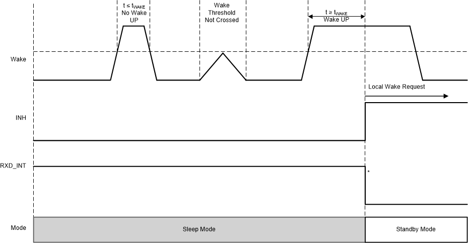
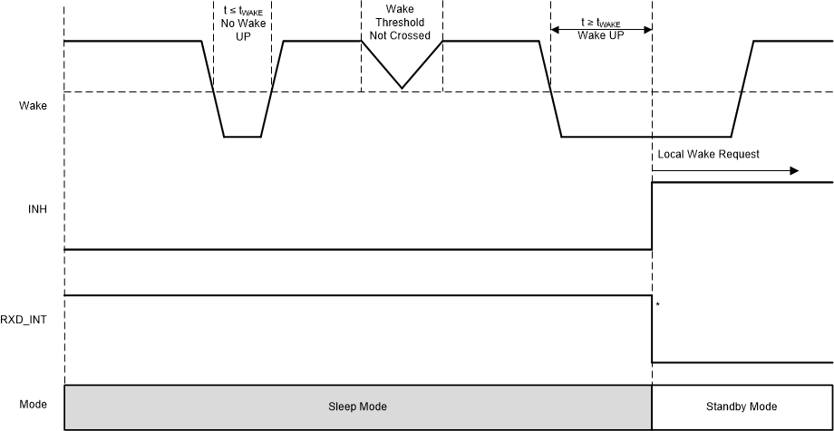
The WAKE terminal is a high voltage input terminal which can be used for local wake-up (LWU) request via a voltage transition. The terminal triggers a LWU event on either a low to high or high to low transition as it has bi-directional input thresholds. This terminal may be used with a switch to VSUP or ground. If the terminal is not used, it should be pulled to ground or VSUP to avoid unwanted wake-up events.
The LWU circuitry is active in sleep mode and standby mode. If a valid LWU event occurs, the device transitions to standby mode. The LWU circuitry is not active in normal mode. To minimize system level current consumption, the internal bias voltages of the terminal follows the state on the terminal. The wake filter time for a valid wake to avoid glitches on wake pin is provided by filter value of tWAKE(MIN). A constant high level on WAKE has an internal pull-up to VSUP and a constant low level on WAKE has an internal pull-down to GND. On power-up, this may look like a LWU event and could be flagged as such.
 Figure 8-8 Local Wake-Up: Rising Edge
 Figure 8-9 Local Wake-Up: Falling Edge
RXD_INT is an internal signal and can be seen in Transceiver test mode when VIO is present.