-
ISO1042 Isolated CAN Transceiver With 70-V Bus Fault Protection and Flexible Data Rate
- 1 Features
- 2 Applications
- 3 Description
- 4 Revision History
- 5 Pin Configuration and Functions
-
6 Specifications
- 6.1 Absolute Maximum Ratings
- 6.2 ESD Ratings
- 6.3 Transient Immunity
- 6.4 Recommended Operating Conditions
- 6.5 Thermal Information
- 6.6 Power Ratings
- 6.7 Insulation Specifications
- 6.8 Safety-Related Certifications
- 6.9 Safety Limiting Values
- 6.10 Electrical Characteristics - DC Specification
- 6.11 Switching Characteristics
- 6.12 Insulation Characteristics Curves
- 6.13 Typical Characteristics
- 7 Parameter Measurement Information
- 8 Detailed Description
- 9 Application and Implementation
- 10Power Supply Recommendations
- 11Layout
- 12Device and Documentation Support
- 13Mechanical, Packaging, and Orderable Information
- IMPORTANT NOTICE
ISO1042 Isolated CAN Transceiver With 70-V Bus Fault Protection and Flexible Data Rate
1 Features
- Meets the ISO 11898-2:2016 physical layer standard
- Supports classic CAN up to 1 Mbps and FD (Flexible Data Rate) up to 5 Mbps
- Low loop delay: 152 ns
- Protection features
- DC bus fault protection voltage: ±70 V
- HBM ESD tolerance on bus pins: ±16 kV
- Driver Dominant Time Out (TXD DTO)
- Undervoltage protection on VCC1 and VCC2
- Common-Mode Voltage Range: ±30 V
- Ideal passive, high impedance bus terminals when unpowered
- High CMTI: 100 kV/µs
- VCC1 voltage range: 1.71 V to 5.5 V
- Supports 1.8-V, 2.5-V, 3.3-V and 5.0-V logic interface to the CAN controller
- VCC2 Voltage Range: 4.5 V to 5.5 V
- Robust Electromagnetic Compatibility (EMC)
- System-level ESD, EFT, and surge immunity
- Low emissions
- Ambient Temperature Range: –40°C to +125°C
- 16-SOIC and 8-SOIC package options
- Automotive version available: ISO1042-Q1
- Safety-related certifications:
- 7071-VPK VIOTM and 1500-VPK VIORM (Reinforced and Basic Options) per DIN VDE V 0884-11:2017-01
- 5000-VRMS Isolation for 1 Minute per UL 1577
- IEC 60950-1, IEC 60601-1 and EN 61010-1 certifications
- CQC, TUV and CSA certifications
3 Description
The ISO1042 device is a galvanically-isolated controller area network (CAN) transceiver that meets the specifications of the ISO11898-2 (2016) standard. The ISO1042 device offers ±70-V DC bus fault protection and ±30-V common-mode voltage range. The device supports up to 5-Mbps data rate in CAN FD mode allowing much faster transfer of payload compared to classic CAN. This device uses a silicon dioxide (SiO2) insulation barrier with a withstand voltage of 5000 VRMS and a working voltage of 1060 VRMS. Electromagnetic compatibility has been significantly enhanced to enable system-level ESD, EFT, surge, and emissions compliance. Used in conjunction with isolated power supplies, the device protects against high voltage, and prevents noise currents from the bus from entering the local ground. The ISO1042 device is available for both basic and reinforced isolation (see Reinforced and Basic Isolation Options). The ISO1042 device supports a wide ambient temperature range of –40°C to +125°C. The device is available in the SOIC-16 (DW) package and a smaller SOIC-8 (DWV) package.
Device Information(1)
| PART NUMBER | PACKAGE | BODY SIZE (NOM) |
|---|---|---|
| ISO1042 | SOIC (8) | 5.85 mm × 7.50 mm |
| SOIC (16) | 10.30 mm × 7.50 mm |
Reinforced and Basic Isolation Options
| FEATURE | ISO1042x | ISO1042Bx |
|---|---|---|
| Protection Level | Reinforced | Basic |
| Surge Test Voltage | 10000 VPK | 6000 VPK |
| Isolation Rating | 5000 VRMS | 5000 VRMS |
| Working Voltage | 1060 VRMS / 1500 VPK | 1060 VRMS / 1500 VPK |
Application Diagram

4 Revision History
Changes from D Revision (October 2019) to E Revision
- Changed new safety certificationGo
Changes from C Revision (October 2018) to D Revision
- Added ISO1042-Q1 linkGo
Changes from B Revision (July 2018) to C Revision
- Initial Release Go
Changes from A Revision (May 2018) to B Revision
- Increased the size of the GND2 plane and changed the NC pin to GND2 in the 16-DW Layout ExampleGo
Changes from * Revision (December 2017) to A Revision
- Changed pin 10 from NC to GND2Go
5 Pin Configuration and Functions
Pin Functions—16 Pins
Pin Functions—8 Pins
| PIN | I/O | DESCRIPTION | |
|---|---|---|---|
| NO. | NAME | ||
| 1 | VCC1 | — | Digital-side supply voltage, Side 1 |
| 2 | TXD | I | CAN transmit data input (LOW for dominant and HIGH for recessive bus states) |
| 3 | RXD | O | CAN receive data output (LOW for dominant and HIGH for recessive bus states) |
| 4 | GND1 | — | Digital-side ground connection, Side 1 |
| 5 | GND2 | — | Transceiver-side ground connection, Side 2 |
| 6 | CANL | I/O | Low-level CAN bus line |
| 7 | CANH | I/O | High-level CAN bus line |
| 8 | VCC2 | — | Transceiver-side supply voltage, Side 2 |
6 Specifications
6.1 Absolute Maximum Ratings
Over operating free-air temperature range (unless otherwise noted)(1)(2)| MIN | MAX | UNIT | ||
|---|---|---|---|---|
| VCC1 | Supply voltage, side 1 | -0.5 | 6 | V |
| VCC2 | Supply voltage, side 2 | -0.5 | 6 | V |
| VIO | Logic input and output voltage range (TXD and RXD) | -0.5 | VCC1+0.5(3) | V |
| IO | Output current on RXD pin | -15 | 15 | mA |
| VBUS | Voltage on bus pins (CANH, CANL) | -70 | 70 | V |
| VBUS_DIFF | Differential voltage on bus pins (CANH-CANL) | -70 | 70 | V |
| TJ | Junction temperature | -40 | 150 | ℃ |
| TSTG | Storage temperature | -65 | 150 | ℃ |
6.2 ESD Ratings
| VALUE | UNIT | |||
|---|---|---|---|---|
| V(ESD) | Electrostatic discharge
Human body model (HBM), per ANSI/ESDA/JEDEC JS-001 |
All pins(1) | ±6000 | V |
| CANH and CANL to GND2(1) | ±16000 | V | ||
| Electrostatic discharge
Charged device model (CDM), per JEDEC specification JESD22-C101 |
All pins(2) | ±1500 | ||
6.3 Transient Immunity
| PARAMETER | TEST CONDITIONS | VALUE | UNIT | |
|---|---|---|---|---|
| VPULSE | ISO7637-2 Transients according to GIFT - ICT CAN EMC test specification | Pulse 1; CAN bus terminals (CANH, CANL) to GND2 | -100 | V |
| Pulse 2; CAN bus terminals (CANH, CANL) to GND2 | 75 | V | ||
| Pulse 3a; CAN bus terminals (CANH, CANL) to GND2 | -150 | V | ||
| Pulse 3b; CAN bus terminals (CANH, CANL) to GND2 | 100 | V | ||
6.4 Recommended Operating Conditions
| MIN | MAX | UNIT | ||
|---|---|---|---|---|
| VCC1 | Supply Voltage, Side 1, 1.8-V operation | 1.71 | 1.89 | V |
| Supply Voltage, Side 1, 2.5-V, 3.3-V and 5.5-V operation | 2.25 | 5.5 | V | |
| VCC2 | Supply Voltage, Side 2 | 4.5 | 5.5 | V |
| TA | Operating ambient temperature | -40 | 125 | °C |
6.5 Thermal Information
| THERMAL METRIC(1) | ISO1042 | UNIT | ||
|---|---|---|---|---|
| DW (SOIC) | DWV (SOIC) | |||
| 16 PINS | 8 PINS | |||
| RΘJA | Junction-to-ambient thermal resistance | 69.9 | 100 | °C/W |
| RΘJC(top) | Junction-to-case (top) thermal resistance | 31.8 | 40.8 | °C/W |
| RΘJB | Junction-to-board thermal resistance | 29.0 | 51.8 | °C/W |
| ΨJT | Junction-to-top characterization parameter | 13.2 | 16.8 | °C/W |
| ΨJB | Junction-to-board characterization parameter | 28.6 | 49.8 | °C/W |
| RΘJC(bot) | Junction-to-case (bottom) thermal resistance | - | - | °C/W |
6.6 Power Ratings
| PARAMETER | TEST CONDITIONS | MIN | TYP | MAX | UNIT | |
|---|---|---|---|---|---|---|
| PD | Maximum power dissipation (both sides) | See Figure 17, VCC1 = VCC2 = 5.5 V, TJ = 150°C, RL = 50 Ω, A repetitive pattern on TXD with 1 ms time period, 990 µs LOW time, and 10 µs HIGH time. | 385 | mW | ||
| PD1 | Maximum power dissipation (side-1) | See Figure 19, VCC1 = VCC2 = 5.5 V, TJ = 150°C, RL = 50 Ω, Input a 2-V pk-pk 2.5-MHz 50% duty cycle differential square wave on CANH-CANL | 25 | mW | ||
| PD2 | Maximum power dissipation (side-2) | See Figure 17, VCC1 = VCC2 = 5.5 V, TJ = 150°C, RL = 50 Ω, A repetitive pattern on TXD with 1 ms time period, 990 µs LOW time, and 10 µs HIGH time. | 360 | mW | ||
6.7 Insulation Specifications
| PARAMETER | TEST CONDITIONS | SPECIFICATIONS | UNIT | ||
|---|---|---|---|---|---|
| DW-16 | DWV-8 | ||||
| IEC 60664-1 | |||||
| CLR | External clearance(1) | Side 1 to side 2 distance through air | >8 | >8.5 | mm |
| CPG | External Creepage(1) | Side 1 to side 2 distance across package surface | >8 | >8.5 | mm |
| DTI | Distance through the insulation | Minimum internal gap (internal clearance) | >17 | >17 | µm |
| CTI | Comparative tracking index | IEC 60112; UL 746A | >600 | >600 | V |
| Material Group | According to IEC 60664-1 | I | I | ||
| Overvoltage category | Rated mains voltage ≤ 600 VRMS | I-IV | I-IV | ||
| Rated mains voltage ≤ 1000 VRMS | I-III | I-III | |||
| DIN VDE V 0884-11:2017-01(2) | |||||
| VIORM | Maximum repetitive peak isolation voltage | AC voltage (bipolar) | 1500 | 1500 | VPK |
| VIOWM | Maximum isolation working voltage | AC voltage (sine wave); time-dependent dielectric breakdown (TDDB) test; | 1060 | 1060 | VRMS |
| DC voltage | 1500 | 1500 | VDC | ||
| VIOTM | Maximum transient isolation voltage | VTEST = VIOTM, t = 60 s (qualification); VTEST = 1.2 × VIOTM, t = 1 s (100% production) | 7071 | 7071 | VPK |
| VIOSM | Maximum surge isolation voltage
ISO1042(3) |
Test method per IEC 62368-1, 1.2/50 µs waveform, VTEST = 1.6 × VIOSM = 10000 VPK (qualification) | 6250 | 6250 | VPK |
| Maximum surge isolation voltage
ISO1042B(3) |
Test method per IEC 62368-1, 1.2/50 µs waveform, VTEST = 1.3 × VIOSM = 6000 VPK (qualification) | 4615 | 4615 | VPK | |
| qpd | Apparent charge(4) | Method a: After I/O safety test subgroup 2/3, Vini = VIOTM, tini = 60 s; Vpd(m) = 1.2 × VIORM, tm = 10 s | ≤ 5 | ≤ 5 | pC |
| Method a: After environmental tests subgroup 1, Vini = VIOTM, tini = 60 s;
ISO1042: Vpd(m) = 1.6 × VIORM, tm = 10 s ISO1042B: Vpd(m) = 1.2 × VIORM, tm = 10 s |
≤ 5 | ≤ 5 | |||
| Method b1: At routine test (100% production) and preconditioning (type test), Vini = VIOTM, tini = 1 s;
ISO1042: Vpd(m) = 1.875 × VIORM, tm = 1 s ISO1042B: Vpd(m) = 1.5 × VIORM, tm = 1 s |
≤ 5 | ≤ 5 | |||
| CIO | Barrier capacitance, input to output(5) | VIO = 0.4 × sin (2 πft), f = 1 MHz | 1 | 1 | pF |
| RIO | Insulation resistance, input to output(5) | VIO = 500 V, TA = 25°C | > 1012 | > 1012 | Ω |
| VIO = 500 V, 100°C ≤ TA ≤ 150°C | > 1011 | > 1011 | |||
| VIO = 500 V at TS = 150°C | > 109 | > 109 | |||
| Pollution degree | 2 | 2 | |||
| Climatic category | 40/125/
21 |
40/125/
21 |
|||
| UL 1577 | |||||
| VISO | Withstand isolation voltage | VTEST = VISO , t = 60 s (qualification); VTEST = 1.2 × VISO , t = 1 s (100% production) | 5000 | 5000 | VRMS |
6.8 Safety-Related Certifications
| VDE | CSA | UL | CQC | TUV |
|---|---|---|---|---|
| Certified according to DIN VDE V 0884-11:2017- 01 | Certified according to IEC 60950-1, IEC 62368-1 and IEC 60601-1 | Recognized under UL 1577 Component Recognition Program | Certified according to GB4943.1-2011 | Certified according to EN 61010-1:2010/A1:2019, EN 60950-1:2006/A2:2013 and EN 62368-1:2014 |
| Maximum transient isolation voltage,
7071 VPK; Maximum repetitive peak isolation voltage, 1500 VPK; Maximum surge isolation voltage, ISO1042: 6250 VPK (Reinforced) ISO1042B: 4615 VPK (Basic) |
CSA 60950-1-07+A1+A2, IEC 60950-1 2nd Ed.+A1+A2 and IEC 62368-1 2nd Ed., for pollution degree 2, material group I
ISO1042: 800 VRMS reinforced isolation ISO1042B: 1060 VRMS basic isolation ---------------- CSA 60601- 1:14 and IEC 60601-1 Ed. 3.1+A1, ISO1042: 2 MOPP (Means of Patient Protection) 250 VRMS (354 VPK) maximum working voltage |
Single protection,
5000 VRMS |
Reinforced insulation, Altitude ≤ 5000 m, Tropical Climate,
700 VRMS maximum working voltage |
EN 61010-1:2010 /A1:2019
ISO1042: 600 VRMS reinforced isolation ISO1042B: 1000 VRMS basic isolation ---------------- EN 60950-1:2006/A2:2013 and EN 62368-1:2014 ISO1042-: 800 VRMS reinforced isolation ISO1042B: 1060 VRMS basic isolation |
| Certificates:
Reinforced: 40040142 Basic: 40047657 |
Master contract number: 220991 | File number: E181974 | Certificate:
CQC15001121716 (DW-16) CQC18001199096 (DWV-8) |
Client ID number: 77311 |
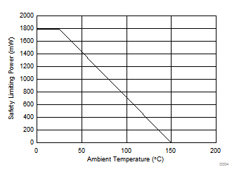
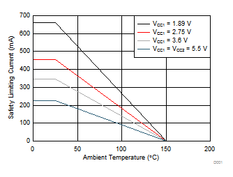
6.9 Safety Limiting Values
Safety limiting(1) intends to minimize potential damage to the isolation barrier upon failure of input or output circuitry.| PARAMETER | TEST CONDITIONS | MIN | TYP | MAX | UNIT | |
|---|---|---|---|---|---|---|
| DW-16 PACKAGE | ||||||
| IS | Safety input, output, or supply current | RθJA = 69.9°C/W, VI = 5.5 V, TJ = 150°C, TA = 25°C, see Figure 1 | 325 | mA | ||
| RθJA = 69.9°C/W, VI = 3.6 V, TJ = 150°C, TA = 25°C, see Figure 1 | 496 | |||||
| RθJA = 69.9°C/W, VI = 2.75 V, TJ = 150°C, TA = 25°C, see Figure 1 | 650 | |||||
| RθJA = 69.9°C/W, VI = 1.89 V, TJ = 150°C, TA = 25°C, see Figure 1 | 946 | |||||
| PS | Safety input, output, or total power | RθJA = 69.9°C/W, TJ = 150°C, TA = 25°C, see Figure 3 | 1788 | mW | ||
| TS | Maximum safety temperature | 150 | °C | |||
| DWV-8 PACKAGE | ||||||
| IS | Safety input, output, or supply current | RθJA = 100°C/W, VI = 5.5 V, TJ = 150°C, TA = 25°C, see Figure 2 | 227 | mA | ||
| RθJA = 100°C/W, VI = 3.6 V, TJ = 150°C, TA = 25°C, see Figure 2 | 347 | |||||
| RθJA = 100°C/W, VI = 2.75 V, TJ = 150°C, TA = 25°C, see Figure 2 | 454 | |||||
| RθJA = 100°C/W, VI = 1.89 V, TJ = 150°C, TA = 25°C, see Figure 2 | 661 | |||||
| PS | Safety input, output, or total power | RθJA = 100°C/W, TJ = 150°C, TA = 25°C, see Figure 4 | 1250 | mW | ||
| TS | Maximum safety temperature | 150 | °C | |||
The junction-to-air thermal resistance, RθJA, in the table is that of a device installed on a high-K test board for leaded surface-mount packages. Use these equations to calculate the value for each parameter:
TJ = TA + RθJA × P, where P is the power dissipated in the device.
TJ(max) = TS = TA + RθJA × PS, where TJ(max) is the maximum allowed junction temperature.
PS = IS × VI, where VI is the maximum input voltage.
6.10 Electrical Characteristics - DC Specification
Over recommended operating conditions (unless otherwise noted)| PARAMETER | TEST CONDITIONS | MIN | TYP | MAX | UNIT | |
|---|---|---|---|---|---|---|
| SUPPLY CHARACTERISTICS | ||||||
| ICC1 | Supply current Side 1 | VCC1 =1.71 V to 1.89 V, TXD = 0 V, bus dominant | 2.3 | 3.5 | mA | |
| VCC1 = 2.25 V to 5.5 V, TXD = 0 V, bus dominant | 2.4 | 3.5 | mA | |||
| VCC1 = 1.71 V to 1.89 V, TXD = VCC1, bus recessive | 1.2 | 2.1 | mA | |||
| VCC1 = 2.25 V to 5.5 V, TXD = VCC1, bus recessive | 1.3 | 2.1 | mA | |||
| ICC2 | Supply current Side 2 | TXD = 0 V, bus dominant, RL = 60 Ω | 43 | 73.4 | mA | |
| TXD = VCC1, bus recessive, RL = 60 Ω | 2.8 | 4.1 | mA | |||
| UVVCC1 | Rising under voltage detection, Side 1 | 1.7 | V | |||
| UVVCC1 | Falling under voltage detection, Side 1 | 1.0 | V | |||
| VHYS(UVCC1) | Hysterisis voltage on VCC1 undervoltage lock-out | 75 | 125 | mV | ||
| UVVCC2 | Rising under voltage detection, side 2 | 4.2 | 4.45 | V | ||
| UVVCC2 | Falling under voltage detection, side 2 | 3.8 | 4.0 | 4.25 | V | |
| VHYS(UVCC2) | Hysterisis voltage on VCC2 undervoltage lock-out | 200 | mV | |||
| TXD TERMINAL | ||||||
| VIH | High level input voltage | 0.7×VCC1 | V | |||
| VIL | Low level input voltage | 0.3×VCC1 | V | |||
| IIH | High level input leakage current | TXD = VCC1 | 1 | uA | ||
| IIL | Low level input leakage current | TXD = 0V | -20 | uA | ||
| CI | Input capacitance | VIN = 0.4 x sin(2 x π x 1E+6 x t) + 2.5 V, VCC1 = 5 V | 3 | pF | ||
| RXD TERMINAL | ||||||
| VOH - VCC1 | High level output voltage | See Figure 18, IO = -4 mA for 4.5 V ≤ VCC1 ≤ 5.5 V | -0.4 | -0.2 | V | |
| See Figure 18, IO = -2 mA for 3.0 V ≤ VCC1 ≤ 3.6 V | -0.2 | -0.07 | V | |||
| See Figure 18, IO = -1 mA for 2.25 V ≤ VCC1 ≤ 2.75 V | -0.1 | -0.04 | V | |||
| See Figure 18, IO = -1 mA for 1.71 V ≤ VCC1 ≤ 1.89 V | -0.1 | -0.045 | V | |||
| VOL | Low level output voltage | See Figure 18, IO = 4 mA for 4.5 V ≤ VCC1 ≤ 5.5 V | 0.2 | 0.4 | V | |
| See Figure 18, IO = 2 mA for 3.0 V ≤ VCC1 ≤ 3.6 V | 0.07 | 0.2 | V | |||
| See Figure 18, IO = 1 mA for 2.25 V ≤ VCC1 ≤ 2.75 V | 0.035 | 0.1 | V | |||
| See Figure 18, IO = 1 mA for 1.71 V ≤ VCC1 ≤ 1.89 V | 0.04 | 0.1 | V | |||
| DRIVER ELECTRICAL CHARACTERISTICS | ||||||
| VO(DOM) | Bus output voltage(Dominant), CANH | See Figure 15 and Figure 16, TXD = 0 V, 50 Ω ≤ RL ≤ 65 Ω, CL = open | 2.75 | 4.5 | V | |
| Bus output voltage(Dominant), CANL | See Figure 15 and Figure 16, TXD = 0 V, 50 Ω ≤ RL ≤ 65 Ω, CL = open | 0.5 | 2.25 | V | ||
| VO(REC) | Bus output voltage(recessive), CANH and CANL | See Figure 15 and Figure 16, TXD = VCC1, RL = open | 2.0 | 0.5 x VCC2 | 3.0 | V |
| VOD(DOM) | Differential output voltage, CANH-CANL (dominant) | See Figure 15 and Figure 16, TXD = 0 V, 45 Ω ≤ RL ≤ 50 Ω, CL = open | 1.4 | 3.0 | V | |
| Differential output voltage, CANH-CANL (dominant) | See Figure 15 and Figure 16, TXD = 0 V, 50 Ω ≤ RL ≤ 65 Ω, CL = open | 1.5 | 3.0 | V | ||
| Differential output voltage, CANH-CANL (dominant) | See Figure 15 and Figure 16, TXD = 0 V, RL = 2240 Ω, CL = open | 1.5 | 5.0 | V | ||
| VOD(REC) | Differential output voltage, CANH-CANL (recessive) | See Figure 15 and Figure 16, TXD = VCC1, RL = 60 Ω, CL = open | -120.0 | 12.0 | mV | |
| Differential output voltage, CANH-CANL (recessive) | See Figure 15 and Figure 16, TXD = VCC1, RL = open, CL = open | -50.0 | 50.0 | mV | ||
| VSYM_DC | DC Output symmetry (VCC2 - VO(CANH) - VO(CANL)) | See Figure 15 and Figure 16, RL = 60 Ω, CL = open, TXD = VCC1 or 0 V | -400.0 | 400.0 | mV | |
| ISO(SS_DOM) | Short circuit current steady state output current, dominant | See Figure 23, VCANH = -5 V to 40 V, CANL = open, TXD = 0 V | -100.0 | mA | ||
| See Figure 23, VCANL = -5 V to 40 V, CANH = open, TXD = 0 V | 100.0 | mA | ||||
| ISO(SS_REC) | Short circuit current steady state output current, recessive | See Figure 23, -27 V ≤ VBUS ≤ 32 V, VBUS = CANH = CANL, TXD = VCC1 | -5.0 | 5.0 | mA | |
| RECEIVER ELECTRICAL CHARACTERISTICS | ||||||
| VIT | Differential input threshold voltage | See Figure 18 and Table 1, |VCM| ≤ 20 V | 500.0 | 900.0 | mV | |
| Differential input threshold voltage | See Figure 18 and Table 1, 20 V ≤ |VCM| ≤ 30 V | 400.0 | 1000.0 | |||
| VHYS | Hysteresis voltage for differential input threshold | See Figure 18 and Table 1 | 120 | |||
| VCM | Input common mode range | See Figure 18 and Table 1 | -30.0 | 30.0 | V | |
| IOFF(LKG) | Power-off bus input leakage current | CANH = CANL = 5 V, VCC2 to GND via 0 Ω and 47 kΩ resistor | 4.8 | uA | ||
| CI | Input capacitance to ground (CANH or CANL) | TXD = VCC1 | 24.0 | 30 | pF | |
| CID | Differential input capacitance (CANH-CANL) | TXD = VCC1 | 12.0 | 15 | pF | |
| RID | Differential input resistance | TXD = VCC1 ; -30 V ≤ VCM ≤ +30 V | 30.0 | 80.0 | kΩ | |
| RIN | Input resistance (CANH or CANL) | TXD = VCC1 ; -30 V ≤ VCM ≤ +30 V | 15.0 | 40.0 | kΩ | |
| RIN(M) | Input resistance matching: (1 - RIN(CANH)/RIN(CANL)) x 100% | VCANH = VCANL = 5 V | -2.0 | 2.0 | % | |
| THERMAL SHUTDOWN | ||||||
| TTSD | Thermal shutdown temperature | 170 | ℃ | |||
| TTSD_HYST | Thermal shutdown hysteresis | 5 | ℃ | |||
6.11 Switching Characteristics
Over recommended operating conditions (unless otherwise noted)| PARAMETER | TEST CONDITIONS | MIN | TYP | MAX | UNIT | |
|---|---|---|---|---|---|---|
| DEVICE SWITCHING CHARACTERISTICS | ||||||
| tPROP(LOOP1) | Total loop delay, driver input TXD to receiver RXD, recessive to dominant | See Figure 20, RL = 60 Ω, CL = 100 pF, CL(RXD) = 15 pF; input rise/fall time (10% to 90%) on TXD =1 ns; 1.71 V ≤ VCC1 ≤ 1.89 V | 70 | 125 | 198.0 | ns |
| See Figure 20, RL = 60 Ω, CL = 100 pF, CL(RXD) = 15 pF; input rise/fall time (10% to 90%) on TXD =1 ns; 2.25 V ≤ VCC1 ≤ 5.5 V | 70 | 122 | 192.0 | ns | ||
| tPROP(LOOP2) | Total loop delay, driver input TXD to receiver RXD, dominant to recessive | See Figure 20, RL = 60 Ω, CL = 100 pF, CL(RXD) = 15 pF; input rise/fall time (10% to 90%) on TXD =1 ns; 1.71 V ≤ VCC1 ≤ 1.89 V | 70 | 155 | 215.0 | ns |
| See Figure 20, RL = 60 Ω, CL = 100 pF, CL(RXD) = 15 pF; input rise/fall time (10% to 90%) on TXD =1 ns; 2.25 V ≤ VCC1 ≤ 5.5 V | 70 | 152 | 215.0 | ns | ||
| tUV_RE_ENABLE | Re-enable time after Undervoltage event | Time for device to return to normal operation from VCC1 or VCC2 under voltage event | 300.0 | µs | ||
| CMTI | Common mode transient immunity | VCM = 1200 VPK, See Figure 24 | 85 | 100 | kV/µs | |
| DRIVER SWITCHING CHARACTERISTICS | ||||||
| tpHR | Propagation delay time, HIGH TXD to driver recessive | See Figure 17, RL = 60 Ω and CL = 100 pF; input rise/fall time (10% to 90%) on TXD =1 ns | 76 | 120 | ns | |
| tpLD | Propagation delay time, LOW TXD to driver dominant | 61 | 120 | |||
| tsk(p) | Pulse skew (|tpHR - tpLD|) | 14 | ||||
| tR | Differential output signal rise time | 45 | ||||
| tF | Differential output signal fall time | 45 | ||||
| VSYM | Output symmetry (dominant or recessive) (VO(CANH) + VO(CANL)) / VCC2 | See Figure 17 and Figure 31 , RTERM = 60 Ω, CSPLIT = 4.7 nF, CL = open, RL = open, TXD = 250 kHz, 1 MHz | 0.9 | 1.1 | V/V | |
| tTXD_DTO | Dominant time out | See Figure 22, RL = 60 Ω and CL = open | 1.2 | 3.8 | ms | |
| RECEIVER SWITCHING CHARACTERISTICS | ||||||
| tpRH | Propagation delay time, bus recessive input to RXD high output | See Figure 19, CL(RXD) = 15 pF | 75 | 130 | ns | |
| tpDL | Propogation delay time, bus dominant input to RXD low output | 63 | 130 | ns | ||
| tR | Output signal rise time(RXD) | 1.4 | ns | |||
| tF | Output signal fall time(RXD) | 1.8 | ns | |||
| FD TIMING PARAMETERS | ||||||
| tBIT(BUS) | Bit time on CAN bus output pins with tBIT(TXD) = 500 ns | See Figure 21, RL = 60 Ω, CL = 100 pF, CL(RXD) = 15 pF; input rise/fall time (10% to 90%) on TXD =1 ns | 435.0 | 530.0 | ns | |
| Bit time on CAN bus output pins with tBIT(TXD) = 200 ns | See Figure 21, RL = 60 Ω, CL = 100 pF, CL(RXD) = 15 pF; input rise/fall time (10% to 90%) on TXD =1 ns | 155.0 | 210.0 | ns | ||
| tBIT(RXD) | Bit time on RXD output pins with tBIT(TXD) = 500 ns | See Figure 21, RL = 60 Ω, CL = 100 pF, CL(RXD) = 15 pF; input rise/fall time (10% to 90%) on TXD =1 ns | 400 | 550.0 | ns | |
| Bit time on RXD output pins with tBIT(TXD) = 200 ns | See Figure 21, RL = 60 Ω, CL = 100 pF, CL(RXD) = 15 pF; input rise/fall time (10% to 90%) on TXD =1 ns | 120.0 | 220.0 | ns | ||
| ∆tREC | Receiver timing symmetry with tBIT(TXD) = 500 ns | See Figure 21, RL = 60 Ω, CL = 100 pF, CL(RXD) = 15 pF; input rise/fall time (10% to 90%) on TXD =1 ns; ΔtREC = tBIT(RXD) - tBIT(BUS) | -65.0 | 40.0 | ns | |
| Receiver timing symmetry with tBIT(TXD) = 200 ns | See Figure 21, RL = 60 Ω, CL = 100 pF, CL(RXD) = 15 pF; input rise/fall time (10% to 90%) on TXD =1 ns; ΔtREC = tBIT(RXD) - tBIT(BUS) | -45.0 | 15.0 | ns | ||
6.12 Insulation Characteristics Curves


6.13 Typical Characteristics

| VCC1 = 5 V | RL = 60 Ω | CL(RXD) = 15 pF |
| Temp = 25°C |

| VCC1 = VCC2 = 5 V | RL = 60 Ω | CL(RXD) = 15 pF |

| VCC1 = VCC2 = 5 V | RL = 60 Ω | CL(RXD) = 15 pF |

| VCC1 = 5 V | RL = 60 Ω | |
| CL = Open | Temp = 25°C |

| TXD = VCC1 | RL = 60 Ω | VCC1 = VCC2 = 5 V |

| VCC2 = 5 V | RL = 60 Ω | CL(RXD) = 15 pF |
| Temp = 25°C |

| VCC1 = VCC2 = 5 V | RL = 60 Ω | CL(RXD) = 15 pF |
| Temp = 25°C |

| VCC = 5 V | VCC1 = 5 V | RL = 60 Ω |
| CL = Open |

| VCC1 = VCC2 = 5 V | RL = 60 Ω | CL = 100 pF |
| CL(RXD) = 15 pF |

| TXD = VCC1 | RL = 60 Ω | VCC1 = VCC2 = 5 V |
7 Parameter Measurement Information
7.1 Test Circuits
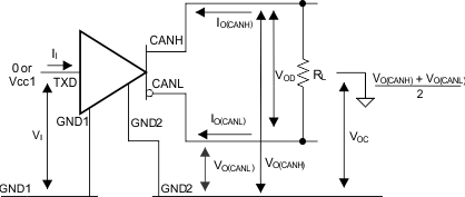 Figure 15. Driver Voltage, Current and Test Definitions
  Figure 16. Bus Logic State Voltage Definitions
tr ≤ 6 ns, tf ≤ 6 ns, ZO = 50 Ω.
 Figure 18. Receiver Voltage and Current Definitions
tr ≤ 6 ns, tf ≤ 6 ns, ZO = 50 Ω.
Table 1. Receiver Differential Input Voltage Threshold Test
| INPUT | OUTPUT | |||
|---|---|---|---|---|
| VCANH | VCANL | |VID| | RXD | |
| -29.5 V | -30.5 V | 1000 mV | L | VOL |
| 30.5 V | 29.5 V | 1000 mV | L | |
| -19.55 V | -20.45 V | 900 mV | L | |
| 20.45 V | 19.55 V | 900 mV | L | |
| -19.75 V | -20.25 V | 500 mV | H | VOH |
| 20.25 V | 19.75 V | 500 mV | H | |
| -29.8 V | -30.2 V | 400 mV | H | |
| 30.2 V | 29.8 V | 400 mV | H | |
| Open | Open | X | H | |
 Figure 20. tLOOP Test Circuit and Voltage Waveforms
  Figure 21. CAN FD Timing Parameter Measurement
 Figure 23. Driver Short-Circuit Current Test Circuit and Waveforms
 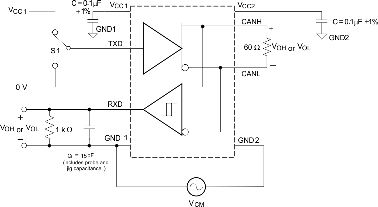 Figure 24. Common-Mode Transient Immunity Test Circuit
 8 Detailed Description
8.1 Overview
The ISO1042 device is a digitally isolated CAN transceiver that offers ±70-V DC bus fault protection and ±30-V common-mode voltage range. The device supports up to 5-Mbps data rate in CAN FD mode allowing much faster transfer of payload compared to classic CAN. The ISO1042 device has an isolation withstand voltage of 5000 VRMS and is available in basic and reinforced isolation with a surge test voltage of 6 kVPK and 10 kVPK respectively. The device can operate from 1.8-V, 2.5-V, 3.3-V, and 5-V supplies on side 1 and a 5-V supply on side 2. This supply range is of particular advantage for applications operating in harsh industrial environments because the low voltage on side 1 enables the connection to low-voltage microcontrollers for power conservation, whereas the 5 V on side 2 maintains a high signal-to-noise ratio of the bus signals.
8.2 Functional Block Diagram

8.3 Feature Description
8.3.1 CAN Bus States
The CAN bus has two states during operation: dominant and recessive. A dominant bus state, equivalent to logic low, is when the bus is driven differentially by a driver. A recessive bus state is when the bus is biased to a common mode of VCC / 2 through the high-resistance internal input resistors of the receiver, equivalent to a logic high. The host microprocessor of the CAN node uses the TXD pin to drive the bus and receives data from the bus on the RXD pin. See Figure 25 and Figure 26.
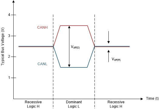 Figure 25. Bus States (Physical Bit Representation)
 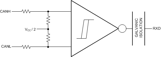 Figure 26. Simplified Recessive Common Mode Bias and Receiver
 8.3.2 Digital Inputs and Outputs: TXD (Input) and RXD (Output)
The VCC1 supply for the isolated digital input and output side of the device can be supplied by 1.8-V, 2.5-V, 3.3-V, and 5-V supplies and therefore the digital inputs and outputs are 1.8-V, 2.5-V, 3.3-V, and 5-V compatible.
NOTE
The TXD pin is very weakly internally pulled up to VCC1. An external pullup resistor should be used to make sure that the TXD pin is biased to recessive (high) level to avoid issues on the bus if the microprocessor does not control the pin and the TXD pin floats. The TXD pullup strength and CAN bit timing require special consideration when the device is used with an open-drain TXD output on the CAN controller of the microprocessor. An adequate external pullup resistor must be used to make sure that the TXD output of the microprocessor maintains adequate bit timing input to the input on the transceiver.
8.3.3 Protection Features
8.3.3.1 TXD Dominant Timeout (DTO)
The TXD DTO circuit prevents the transceiver from blocking network communication in the event of a hardware or software failure where the TXD pin is held dominant longer than the timeout period, tTXD_DTO. The DTO circuit timer starts on a falling edge on the TXD pin. The DTO circuit disables the CAN bus driver if no rising edge occurs before the timeout period expires, which frees the bus for communication between other nodes on the network. The CAN driver is activated again when a recessive signal occurs on the TXD pin, clearing the TXD DTO condition. The receiver and RXD pin still reflect activity on the CAN bus, and the bus terminals are biased to the recessive level during a TXD dominant timeout.
 Figure 27. Example Timing Diagram for TXD DTO
 NOTE
The minimum dominant TXD time (tTXD_DTO) allowed by the TXD DTO circuit limits the minimum possible transmitted data rate of the device. The CAN protocol allows a maximum of eleven successive dominant bits (on TXD) for the worst case, where five successive dominant bits are followed immediately by an error frame. This, along with the tTXD_DTO minimum, limits the minimum data rate. Calculate the minimum transmitted data rate with Equation 1.
8.3.3.2 Thermal Shutdown (TSD)
If the junction temperature of the device exceeds the thermal shutdown threshold (TTSD), the device turns off the CAN driver circuits, blocking the TXD-to-bus transmission path. The CAN bus terminals are biased to the recessive level during a thermal shutdown, and the receiver-to-RXD path remains operational. The shutdown condition is cleared when the junction temperature drops at least the thermal shutdown hysteresis temperature (TTSD_HYST) below the thermal shutdown temperature (TTSD) of the device.
8.3.3.3 Undervoltage Lockout and Default State
The supply pins have undervoltage detection that places the device in protected or default mode which protects the bus during an undervoltage event on the VCC1 or VCC2 supply pins. If the bus-side power supply, VCC2, is less than about 4 V, the power shutdown circuits in the ISO1042 device disable the transceiver to prevent false transmissions because of an unstable supply. If the VCC1 supply is still active when this occurs, the receiver output (RXD) goes to a default HIGH (recessive) value. Table 2 summarizes the undervoltage lockout and fail-safe behavior.
Table 2. Undervoltage Lockout and Default State
| VCC1 | VCC2 | DEVICE STATE | BUS OUTPUT | RXD |
|---|---|---|---|---|
| > UVVCC1 | > UVVCC2 | Functional | Per Device State and TXD | Mirrors Bus |
| <UVVCC1 | > UVVCC2 | Protected | Recessive | Undetermined |
| >UVVCC1 | < UVVCC2 | Protected | High Impedance | Recessive (Default High) |
NOTE
After an undervoltage condition is cleared and the supplies have returned to valid levels, the device typically resumes normal operation in 300 µs.
8.3.3.4 Floating Pins
Pullup and pulldown resistors should be used on critical pins to place the device into known states if the pins float. The TXD pin should be pulled up through a resistor to the VCC1 pin to force a recessive input level if the microprocessor output to the pin floats.
8.3.3.5 Unpowered Device
The device is designed to be ideal passive or no load to the CAN bus if it is unpowered. The bus pins (CANH, CANL) have extremely low leakage currents when the device is unpowered to avoid loading down the bus which is critical if some nodes of the network are unpowered while the rest of the of network remains in operation.
8.3.3.6 CAN Bus Short Circuit Current Limiting
The device has two protection features that limit the short circuit current when a CAN bus line has a short-circuit fault condition. The first protection feature is driver current limiting (both dominant and recessive states) and the second feature is TXD dominant state time out to prevent permanent higher short circuit current of the dominant state during a system fault. During CAN communication the bus switches between dominant and recessive states, therefore the short circuit current may be viewed either as the instantaneous current during each bus state or as an average current of the two states. For system current (power supply) and power considerations in the termination resistors and common-mode choke ratings, use the average short circuit current. Determine the ratio of dominant and recessive bits by the data in the CAN frame plus the following factors of the protocol and PHY that force either recessive or dominant at certain times:
- Control fields with set bits
- Bit stuffing
- Interframe space
- TXD dominant time out (fault case limiting)
These factors ensure a minimum recessive amount of time on the bus even if the data field contains a high percentage of dominant bits. The short circuit current of the bus depends on the ratio of recessive to dominant bits and their respective short circuit currents. Use Equation 2 to calculate the average short circuit current.
where
- IOS(AVG) is the average short circuit current
- %Transmit is the percentage the node is transmitting CAN messages
- %Receive is the percentage the node is receiving CAN messages
- %REC_Bits is the percentage of recessive bits in the transmitted CAN messages
- %DOM_Bits is the percentage of dominant bits in the transmitted CAN messages
- IOS(SS)_REC is the recessive steady state short circuit current
- IOS(SS)_DOM is the dominant steady state short circuit current
NOTE
Consider the short circuit current and possible fault cases of the network when sizing the power ratings of the termination resistance and other network components.
8.4 Device Functional Modes
Table 3 and Table 4 list the driver and receiver functions. Table 5 lists the functional modes for the ISO1042 device.
Table 3. Driver Function Table
| INPUT | OUTPUTS | DRIVEN BUS STATE | |
|---|---|---|---|
| TXD(1) | CANH(1) | CANL(1) | |
| L | H | L | Dominant |
| H | Z | Z | Recessive |
Table 4. Receiver Function Table
| DEVICE MODE | CAN DIFFERENTIAL INPUTS
VID = VCANH – VCANL(3) |
BUS STATE | RXD PIN(1) |
|---|---|---|---|
| Normal | VID ≥ VIT(MAX) | Dominant | L |
| VIT(MIN) < VID < VIT(MAX) | ? | ? | |
| VID ≤ VIT(MIN) | Recessive | H | |
| Open (VID ≈ 0 V) | Open | H |
Table 5. Function Table(1)
| DRIVER | RECEIVER | |||||
|---|---|---|---|---|---|---|
| INPUTS | OUTPUTS | BUS STATE | DIFFERENTIAL INPUTS VID = CANH–CANL(3) | OUTPUT
RXD |
BUS STATE | |
| TXD | CANH | CANL | ||||
| L(2) | H | L | DOMINANT | VID ≥ VIT(MAX) | L | DOMINANT |
| H | Z | Z | RECESSIVE | VIT(MIN) < VID < VIT(MAX) | ? | ? |
| Open | Z | Z | RECESSIVE | VID ≤ VIT(MIN) | H | RECESSIVE |
| X | Z | Z | RECESSIVE | Open (VID ≈ 0 V) | H | RECESSIVE |
9 Application and Implementation
NOTE
Information in the following applications sections is not part of the TI component specification, and TI does not warrant its accuracy or completeness. TI’s customers are responsible for determining suitability of components for their purposes. Customers should validate and test their design implementation to confirm system functionality.
9.1 Application Information
The ISO1042 device can be used with other components from Texas Instruments such as a microcontroller, a transformer driver, and a linear voltage regulator to form a fully isolated CAN interface.
9.2 Typical Application
 Figure 28. Application Circuit With ISO1042 in 16-SOIC Package
  Figure 29. Application Circuit With ISO1042 in 8-SOIC Package
 9.2.1 Design Requirements
Unlike an optocoupler-based solution, which requires several external components to improve performance, provide bias, or limit current, the ISO1042 device only requires external bypass capacitors to operate.
9.2.2 Detailed Design Procedure
9.2.2.1 Bus Loading, Length and Number of Nodes
The ISO 11898-2 Standard specifies a maximum bus length of 40 m and maximum stub length of 0.3 m. However, with careful design, users can have longer cables, longer stub lengths, and many more nodes to a bus. A large number of nodes requires transceivers with high input impedance such as the ISO1042 transceivers.
Many CAN organizations and standards have scaled the use of CAN for applications outside the original ISO 11898-2 Standard. These organizations and standards have made system-level trade-offs for data rate, cable length, and parasitic loading of the bus. Examples of some of these specifications are ARINC825, CANopen, DeviceNet, and NMEA2000.
The ISO1042 device is specified to meet the 1.5-V requirement with a 50-Ω load, incorporating the worst case including parallel transceivers. The differential input resistance of the ISO1042 device is a minimum of 30 kΩ. If 100 ISO1042 transceivers are in parallel on a bus, this requirement is equivalent to a 300-Ω differential load worst case. That transceiver load of 300 Ω in parallel with the 60 Ω gives an equivalent loading of 50 Ω. Therefore, the ISO1042 device theoretically supports up to 100 transceivers on a single bus segment. However, for CAN network design margin must be given for signal loss across the system and cabling, parasitic loadings, network imbalances, ground offsets and signal integrity, therefore a practical maximum number of nodes is typically much lower. Bus length may also be extended beyond the original ISO 11898 standard of 40 m by careful system design and data-rate tradeoffs. For example, CANopen network design guidelines allow the network to be up to 1 km with changes in the termination resistance, cabling, less than 64 nodes, and a significantly lowered data rate.
This flexibility in CAN network design is one of the key strengths of the various extensions and additional standards that have been built on the original ISO 11898-2 CAN standard. Using this flexibility requires the responsibility of good network design and balancing these tradeoffs.
9.2.2.2 CAN Termination
The ISO11898 standard specifies the interconnect to be a single twisted pair cable (shielded or unshielded) with 120-Ω characteristic impedance (ZO). Resistors equal to the characteristic impedance of the line should be used to terminate both ends of the cable to prevent signal reflections. Unterminated drop-lines (stubs) connecting nodes to the bus should be kept as short as possible to minimize signal reflections. The termination may be in a node, but if nodes are removed from the bus, the termination must be carefully placed so that it is not removed from the bus.
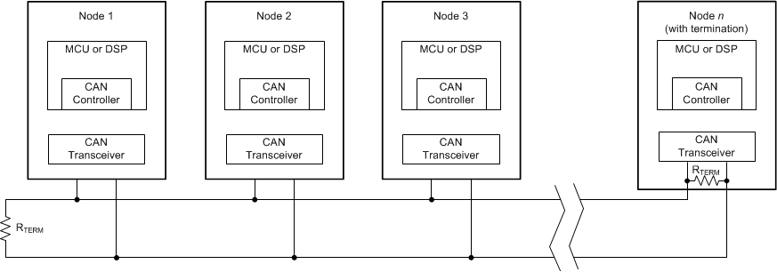 Figure 30. Typical CAN Bus
 Termination may be a single 120-Ω resistor at the end of the bus, either on the cable or in a terminating node. If filtering and stabilization of the common-mode voltage of the bus is desired, then split termination can be used. (See Figure 31). Split termination improves the electromagnetic emissions behavior of the network by eliminating fluctuations in the bus common-mode voltages at the start and end of message transmissions.
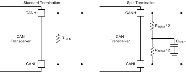 Figure 31. CAN Bus Termination Concepts
 9.2.3 Application Curve

9.3 DeviceNet Application
 Figure 33. ISO1042, ISO1211 and SN6505 Used in a DeviceNet Application
 Figure 33 shows an application circuit for using ISO1042, ISO1211 and SN6505 in a DeviceNet application. ISO1042 is used to isolate the CAN interface. The ISO1211 24-V digital input receiver is used to detect the absence or presence of the 24-V field supply. The SN6505 push-pull transformer driver, is used to create an auxiliary isolated power supply for the micro-controller side using the 24-V field supply.
10 Power Supply Recommendations
To make sure operation is reliable at all data rates and supply voltages, a 0.1-µF bypass capacitor is recommended at the input and output supply pins (VCC1 and VCC2). The capacitors should be placed as close to the supply pins as possible. In addition, a bulk capacitance, typically 4.7 μF, should be placed near the VCC2 supply pin. If only a single primary-side power supply is available in an application, isolated power can be generated for the secondary-side with the help of a transformer driver such as TI's SN6505B. For such applications, detailed power supply design, and transformer selection recommendations are available in the SN6505 Low-Noise 1-A Transformer Drivers for Isolated Power Supplies data sheet.
11 Layout
11.1 Layout Guidelines
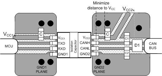
A minimum of four layers is required to accomplish a low EMI PCB design (see Figure 34). Layer stacking should be in the following order (top-to-bottom): high-speed signal layer, ground plane, power plane and low-frequency signal layer.
- Routing the high-speed traces on the top layer avoids the use of vias (and the introduction of their inductances) and allows for clean interconnects between the isolator and the transmitter and receiver circuits of the data link.
- Placing a solid ground plane next to the high-speed signal layer establishes controlled impedance for transmission line interconnects and provides an excellent low-inductance path for the return current flow.
- Placing the power plane next to the ground plane creates additional high-frequency bypass capacitance of approximately 100 pF/in2.
- Routing the slower speed control signals on the bottom layer allows for greater flexibility as these signal links usually have margin to tolerate discontinuities such as vias.
Suggested placement and routing of ISO1042 bypass capacitors and optional TVS diodes is shown in Figure 35 and Figure 36. In particular, place the VCC2 bypass capacitors on the top layer, as close to the device pins as possible, and complete the connection to the VCC2 and GND2 pins without using vias. Note that the SOIC-16 variant needs two VCC2 bypass capacitor, one on each VCC2 pin.
If an additional supply voltage plane or signal layer is needed, add a second power or ground plane system to the stack to keep it symmetrical. This makes the stack mechanically stable and prevents it from warping. Also the power and ground plane of each power system can be placed closer together, thus increasing the high-frequency bypass capacitance significantly.
For detailed layout recommendations, refer to the Digital Isolator Design Guide.
11.1.1 PCB Material
For digital circuit boards operating at less than 150 Mbps, (or rise and fall times greater than 1 ns), and trace lengths of up to 10 inches, use standard FR-4 UL94V-0 printed circuit board. This PCB is preferred over lower-cost alternatives because of lower dielectric losses at high frequencies, less moisture absorption, greater strength and stiffness, and the self-extinguishing flammability-characteristics.
12 Device and Documentation Support
12.1 Documentation Support
12.1.1 Related Documentation
For related documentation see the following:
- Texas Instruments, Digital Isolator Design Guide
- Texas Instruments, ISO1042DW Isolated CAN Transceiver Evaluation Module User's Guide
- Texas Instruments, Isolate your CAN systems without compromising on performance or space TI TechNote
- Texas Instruments, Isolation Glossary
- Texas Instruments, High-voltage reinforced isolation: Definitions and test methodologies
- Texas Instruments, How to Isolate Signal and Power in Isolated CAN Systems TI TechNote
- Texas Instruments, How to Design Isolated CAN Systems With Correct Bus Protection Application Report
12.2 Receiving Notification of Documentation Updates
To receive notification of documentation updates, navigate to the device product folder on ti.com. In the upper right corner, click on Alert me to register and receive a weekly digest of any product information that has changed. For change details, review the revision history included in any revised document.
12.3 Community Resource
TI E2E™ support forums are an engineer's go-to source for fast, verified answers and design help — straight from the experts. Search existing answers or ask your own question to get the quick design help you need.
Linked content is provided "AS IS" by the respective contributors. They do not constitute TI specifications and do not necessarily reflect TI's views; see TI's Terms of Use.
12.4 Trademarks
E2E is a registered trademark of Texas Instruments.
12.5 Electrostatic Discharge Caution

This integrated circuit can be damaged by ESD. Texas Instruments recommends that all integrated circuits be handled with appropriate precautions. Failure to observe proper handling and installation procedures can cause damage.
ESD damage can range from subtle performance degradation to complete device failure. Precision integrated circuits may be more susceptible to damage because very small parametric changes could cause the device not to meet its published specifications.
12.6 Glossary
SLYZ022 — TI Glossary.
This glossary lists and explains terms, acronyms, and definitions.
13 Mechanical, Packaging, and Orderable Information
The following pages include mechanical packaging and orderable information. This information is the most current data available for the designated devices. This data is subject to change without notice and revision of this document. For browser-based versions of this data sheet, refer to the left-hand navigation.
IMPORTANT NOTICE AND DISCLAIMER
| TI PROVIDES TECHNICAL AND RELIABILITY DATA (INCLUDING DATASHEETS), DESIGN RESOURCES (INCLUDING REFERENCE DESIGNS), APPLICATION OR OTHER DESIGN ADVICE, WEB TOOLS, SAFETY INFORMATION, AND OTHER RESOURCES “AS IS” AND WITH ALL FAULTS, AND DISCLAIMS ALL WARRANTIES, EXPRESS AND IMPLIED, INCLUDING WITHOUT LIMITATION ANY IMPLIED WARRANTIES OF MERCHANTABILITY, FITNESS FOR A PARTICULAR PURPOSE OR NON-INFRINGEMENT OF THIRD PARTY INTELLECTUAL PROPERTY RIGHTS. |
| These resources are intended for skilled developers designing with TI products. You are solely responsible for (1) selecting the appropriate TI products for your application, (2) designing, validating and testing your application, and (3) ensuring your application meets applicable standards, and any other safety, security, or other requirements. These resources are subject to change without notice. TI grants you permission to use these resources only for development of an application that uses the TI products described in the resource. Other reproduction and display of these resources is prohibited. No license is granted to any other TI intellectual property right or to any third party intellectual property right. TI disclaims responsibility for, and you will fully indemnify TI and its representatives against, any claims, damages, costs, losses, and liabilities arising out of your use of these resources. |
| TI’s products are provided subject to TI’s Terms of Sale (www.ti.com/legal/termsofsale.html) or other applicable terms available either on ti.com or provided in conjunction with such TI products. TI’s provision of these resources does not expand or otherwise alter TI’s applicable warranties or warranty disclaimers for TI products. |
| Mailing Address: Texas Instruments, Post Office Box 655303, Dallas, Texas 75265
Copyright © 2020, Texas Instruments Incorporated |


