SLLSF22H April   2018  – June 2024 ISO1410 , ISO1412 , ISO1430 , ISO1432 , ISO1450 , ISO1452

PRODUCTION DATA  

  1.   1
  2. Features
  3. Applications
  4. Description
  5. Description Continued
  6. Device Comparison Table
  7. Pin Configuration and Functions
    1.     Pin Functions: Full-Duplex Device
    2.     Pin Functions: Half-Duplex Device
  8. Specifications
    1. 7.1  Absolute Maximum Ratings
    2. 7.2  ESD Ratings
    3. 7.3  Recommended Operating Conditions
    4. 7.4  Thermal Information
    5. 7.5  Power Ratings
    6. 7.6  Insulation Specifications
    7. 7.7  Safety-Related Certifications
    8. 7.8  Safety Limiting Values
    9. 7.9  Electrical Characteristics: Driver
    10. 7.10 Electrical Characteristics: Receiver
    11. 7.11 Supply Current Characteristics: Side 1 (ICC1)
    12. 7.12 Supply Current Characteristics: Side 2 (ICC2)
    13. 7.13 Switching Characteristics: Driver
    14. 7.14 Switching Characteristics: Receiver
    15. 7.15 Insulation Characteristics Curves
    16. 7.16 Typical Characteristics
  9. Parameter Measurement Information
  10. Detailed Description
    1. 9.1 Overview
    2. 9.2 Functional Block Diagram
    3. 9.3 Feature Description
      1. 9.3.1 Electromagnetic Compatibility (EMC) Considerations
      2. 9.3.2 Failsafe Receiver
      3. 9.3.3 Thermal Shutdown
      4. 9.3.4 Glitch-Free Power Up and Power Down
    4. 9.4 Device Functional Modes
      1. 9.4.1 Device I/O Schematics
  11. 10Application and Implementation
    1. 10.1 Application Information
    2. 10.2 Typical Application
      1. 10.2.1 Design Requirements
      2. 10.2.2 Detailed Design Procedure
        1. 10.2.2.1 Data Rate and Bus Length
        2. 10.2.2.2 Stub Length
        3. 10.2.2.3 Bus Loading
      3. 10.2.3 Application Curves
        1. 10.2.3.1 Insulation Lifetime
  12. 11Power Supply Recommendations
  13. 12Layout
    1. 12.1 Layout Guidelines
      1. 12.1.1 PCB Material
    2. 12.2 Layout Example
  14. 13Device and Documentation Support
    1. 13.1 Documentation Support
      1. 13.1.1 Related Documentation
        1. 13.1.1.1 Related Links
    2. 13.2 Receiving Notification of Documentation Updates
    3. 13.3 Support Resources
    4. 13.4 Trademarks
    5. 13.5 Electrostatic Discharge Caution
    6. 13.6 Glossary
  15. 14Revision History
  16. 15Mechanical, Packaging, and Orderable Information

Typical Characteristics

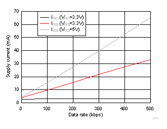
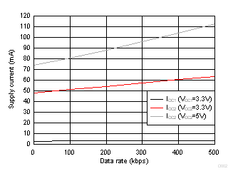
ISO1450 ISO1452 ISO1410 ISO1412 ISO1430 ISO1432 ISO141x Supply Current Vs Data Rate- No Load
DE = VCC1RE = GND1TA = 25°C
Figure 7-3 ISO141x Supply Current Vs Data Rate- No Load
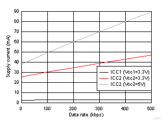
ISO1450 ISO1452 ISO1410 ISO1412 ISO1430 ISO1432 ISO141x Supply Current Vs Data Rate- With 120Ω||50pf Load
DE = VCC1RE = GND1Driver Load = 120 Ω || 50pF
TA = 25°CLoad On R = 15 pF
Figure 7-5 ISO141x Supply Current Vs Data Rate- With 120Ω||50pf Load
ISO1450 ISO1452 ISO1410 ISO1412 ISO1430 ISO1432 ISO143x Supply Current Vs. Data Rate - 120Ω||50pF Load
DE = VCC1TA = 25°CRE = GND1
Driver Load = 120 Ω || 50pF50pF, Load On R = 15pf
Figure 7-7 ISO143x Supply Current Vs. Data Rate - 120Ω||50pF Load
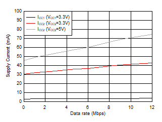
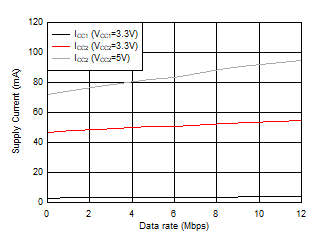
ISO1450 ISO1452 ISO1410 ISO1412 ISO1430 ISO1432 ISO145x Supply Current Vs Data Rate- No Load
DE = VCC1TA = 25°CRE = GND1
Figure 7-9 ISO145x Supply Current Vs Data Rate- No Load
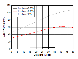
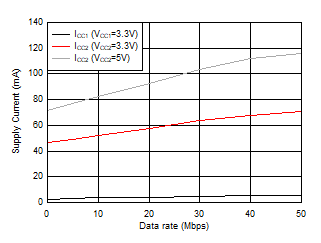
ISO1450 ISO1452 ISO1410 ISO1412 ISO1430 ISO1432 ISO145x Supply Current Vs Data Rate- 54Ω||50pF Load
DE = VCC1TA = 25°CRE = GND1
Driver Load = 54 Ω || 50pF50pF, Load On R = 15pf
Figure 7-11 ISO145x Supply Current Vs Data Rate- 54Ω||50pF Load
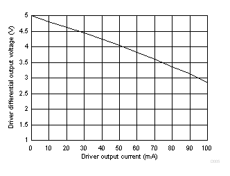
ISO1450 ISO1452 ISO1410 ISO1412 ISO1430 ISO1432 Driver Differential Output Voltage Vs Driver Output Current
DE = VCC1D = GND1VCC1 = 3.3 V
TA = 25°CVCC2 = 5 V
Figure 7-13 Driver Differential Output Voltage Vs Driver Output Current
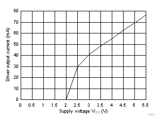
ISO1450 ISO1452 ISO1410 ISO1412 ISO1430 ISO1432 Driver Output Current Vs Supply Voltage (VCC2)
RL = 54 ΩDE = D = VCC1TA = 25°C
Figure 7-15 Driver Output Current Vs Supply Voltage (VCC2)
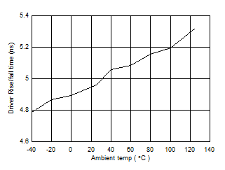
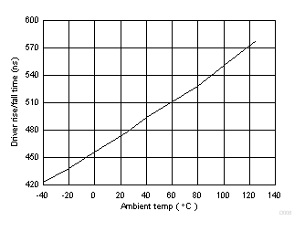
ISO1450 ISO1452 ISO1410 ISO1412 ISO1430 ISO1432 ISO143x Driver Rise/Fall Time (ns) Vs Temperature (C)
VCC1 = 3.3 VVCC2 = 5 V
Figure 7-17 ISO143x Driver Rise/Fall Time (ns) Vs Temperature (C)
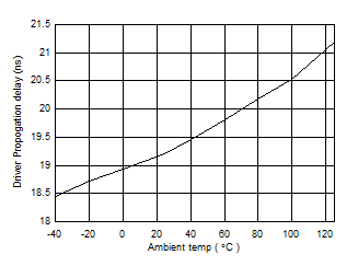
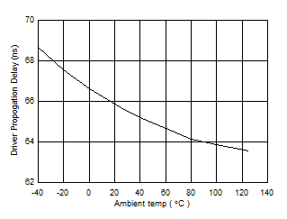
ISO1450 ISO1452 ISO1410 ISO1412 ISO1430 ISO1432 ISO141x Driver Propagation Delay (ns) Vs Temperature (c)
VCC1 = 3.3 VVCC2 = 5 V
Figure 7-19 ISO141x Driver Propagation Delay (ns) Vs Temperature (c)
ISO1450 ISO1452 ISO1410 ISO1412 ISO1430 ISO1432 ISO145x Driver Propagation Delay (ns) Vs Temperature (C)
VCC1 = 3.3 VVCC2 = 5 V
Figure 7-21 ISO145x Driver Propagation Delay (ns) Vs Temperature (C)
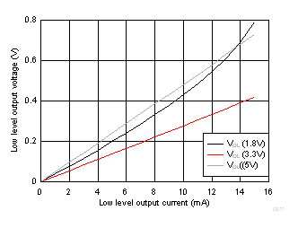
ISO1450 ISO1452 ISO1410 ISO1412 ISO1430 ISO1432 Receiver Buffer Low Level Output Voltage Vs Low Level Output Current
TA = 25°C
Figure 7-23 Receiver Buffer Low Level Output Voltage Vs Low Level Output Current
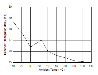
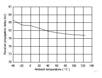
ISO1450 ISO1452 ISO1410 ISO1412 ISO1430 ISO1432 ISO143x Receiver Propagation Delay (ns) Vs. Temperature (C)
VCC1 = 3.3 VVCC2 = 5 V
Figure 7-25 ISO143x Receiver Propagation Delay (ns) Vs. Temperature (C)
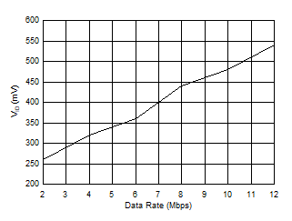
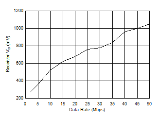
ISO1450 ISO1452 ISO1410 ISO1412 ISO1430 ISO1432 ISO143x Receiver VID vs Signaling Rate
For PWD ≤±5%
Figure 7-27 ISO143x Receiver VID vs Signaling Rate
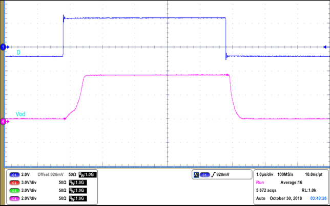
ISO1450 ISO1452 ISO1410 ISO1412 ISO1430 ISO1432 ISO141x Driver Propagation Delay
VCC1 = 3.3 V VCC2 = 5 V TA = 25° C
DE = VCC1
Figure 7-29 ISO141x Driver Propagation Delay
ISO1450 ISO1452 ISO1410 ISO1412 ISO1430 ISO1432 ISO145x Driver Propagation Delay
VCC1 = 3.3 V VCC2 = 5 V TA = 25° C
DE = VCC1
Figure 7-31 ISO145x Driver Propagation Delay
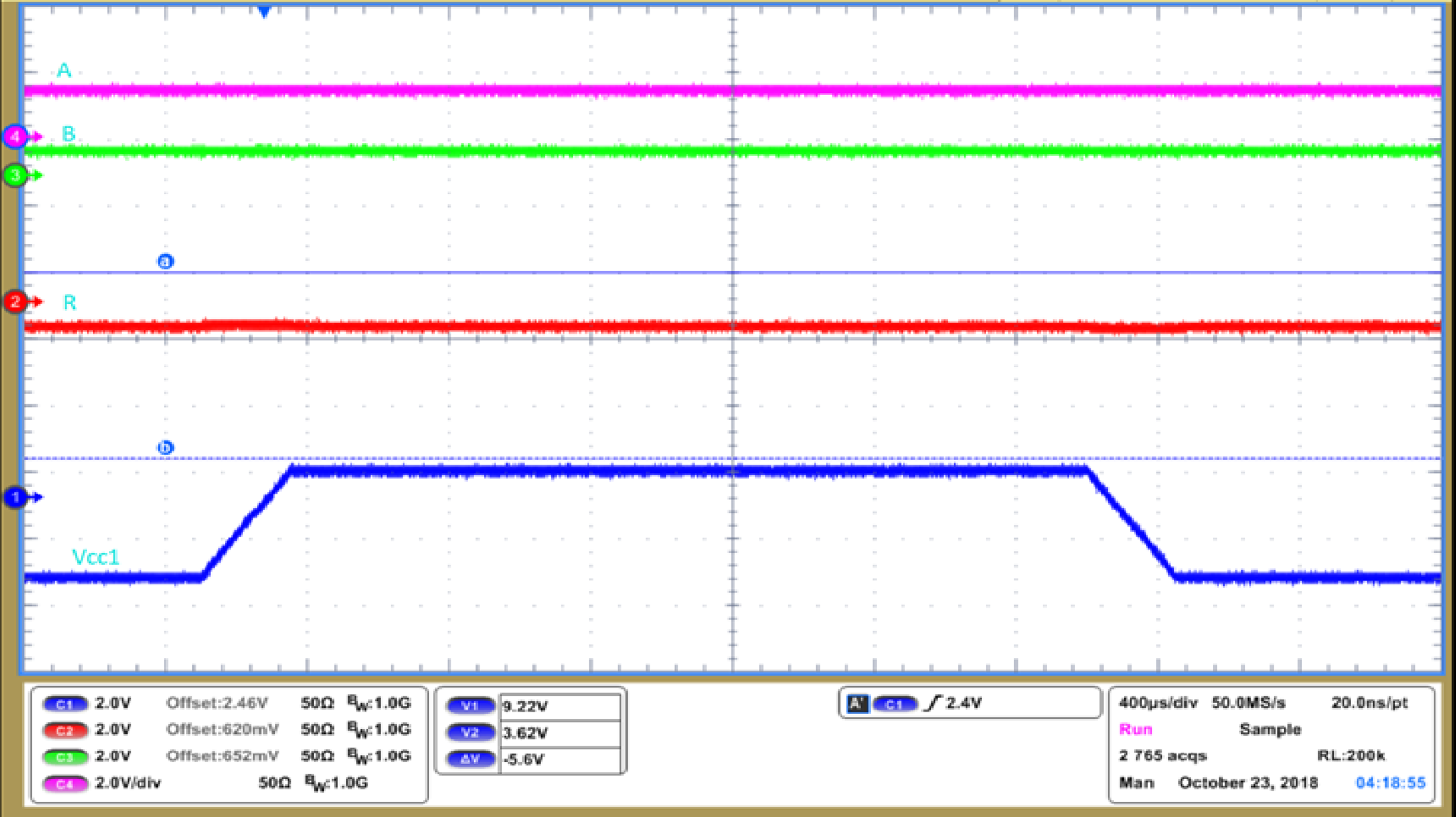
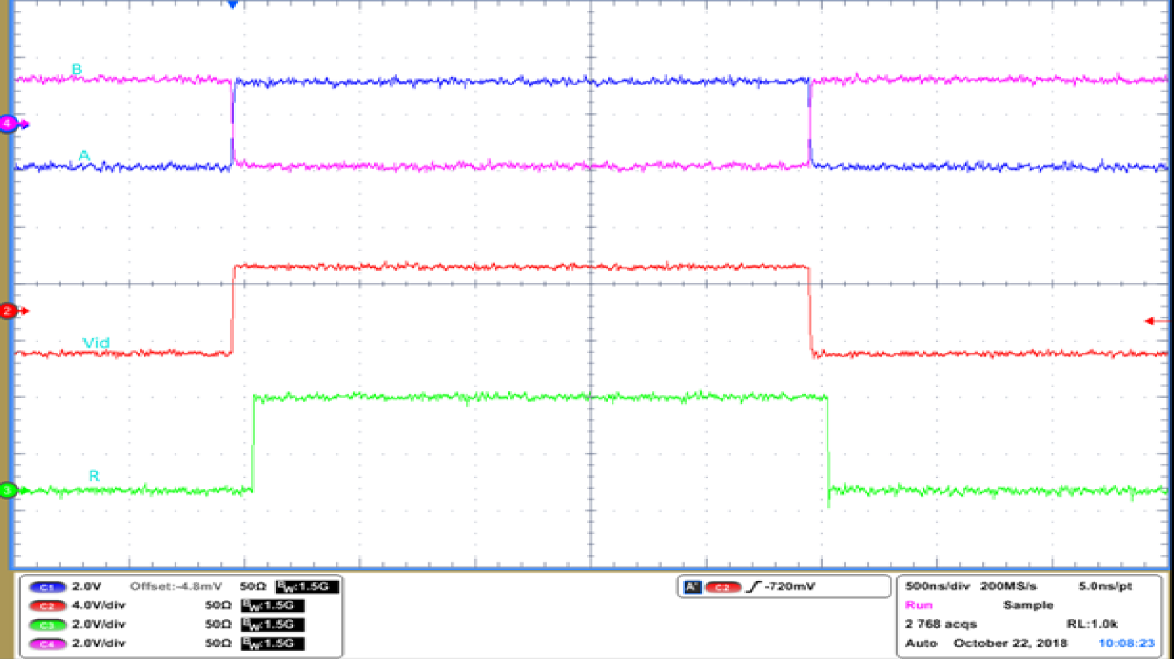
ISO1450 ISO1452 ISO1410 ISO1412 ISO1430 ISO1432 VCC1 Power Up/Power Down - Glitch Free Behavior
Figure 7-33 VCC1 Power Up/Power Down - Glitch Free Behavior
ISO1450 ISO1452 ISO1410 ISO1412 ISO1430 ISO1432 ISO141x Supply Current Vs Data Rate- With 54Ω||50pf Load
DE = VCC1RE = GND1Driver Load = 54 Ω || 50pF
TA = 25°CLoad On R = 15 pF
Figure 7-4 ISO141x Supply Current Vs Data Rate- With 54Ω||50pf Load
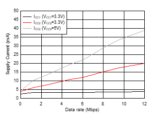
ISO1450 ISO1452 ISO1410 ISO1412 ISO1430 ISO1432 ISO143x Supply Current Vs. Data Rate - No Load
DE = VCC1TA = 25°CRE = GND1
Figure 7-6 ISO143x Supply Current Vs. Data Rate - No Load
ISO1450 ISO1452 ISO1410 ISO1412 ISO1430 ISO1432 ISO143x Supply Current Vs Data Rate- 54Ω||50pF Load
DE = VCC1TA = 25°CRE = GND1
Driver Load = 54 Ω || 50pF50pF, Load On R = 15pf
Figure 7-8 ISO143x Supply Current Vs Data Rate- 54Ω||50pF Load
ISO1450 ISO1452 ISO1410 ISO1412 ISO1430 ISO1432 ISO145x Supply Current Vs Data Rate- 120Ω||50pF Load
DE = VCC1TA = 25°CRE = GND1
Driver Load = 120 Ω || 50pF50pF, Load On R = 15pf
Figure 7-10 ISO145x Supply Current Vs Data Rate- 120Ω||50pF Load
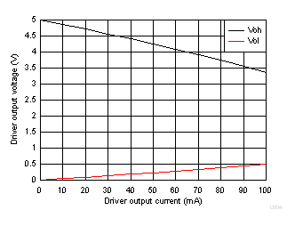
ISO1450 ISO1452 ISO1410 ISO1412 ISO1430 ISO1432 Driver Output Voltage Vs Driver Output Current
DE = VCC1D = GND1VCC1 = 3.3 V
TA = 25°CVCC2 = 5 V
Figure 7-12 Driver Output Voltage Vs Driver Output Current
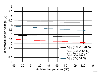
ISO1450 ISO1452 ISO1410 ISO1412 ISO1430 ISO1432 Driver Differential Output Voltage Vs Temperature
Figure 7-14 Driver Differential Output Voltage Vs Temperature
ISO1450 ISO1452 ISO1410 ISO1412 ISO1430 ISO1432 ISO141x Driver Rise/fall Time (ns) Vs Temperature (c)
VCC1 = 3.3 VVCC2 = 5 V
Figure 7-16 ISO141x Driver Rise/fall Time (ns) Vs Temperature (c)
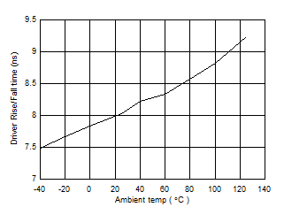
ISO1450 ISO1452 ISO1410 ISO1412 ISO1430 ISO1432 ISO145x Driver Rise/Fall Time (ns) Vs Temperature (C)
VCC1 = 3.3 VVCC2 = 5 V
Figure 7-18 ISO145x Driver Rise/Fall Time (ns) Vs Temperature (C)
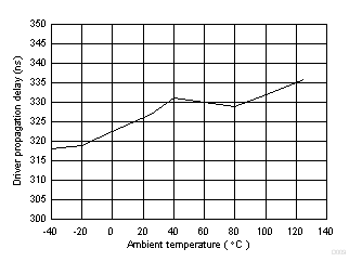
ISO1450 ISO1452 ISO1410 ISO1412 ISO1430 ISO1432 ISO143x Driver Propagation Delay (ns) Vs Temperature (C)
VCC1 = 3.3 VVCC2 = 5 V
Figure 7-20 ISO143x Driver Propagation Delay (ns) Vs Temperature (C)
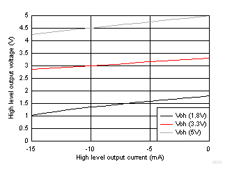
ISO1450 ISO1452 ISO1410 ISO1412 ISO1430 ISO1432 Receiver Buffer High Level Output Voltage Vs High Level Output Current
TA = 25° C
Figure 7-22 Receiver Buffer High Level Output Voltage Vs High Level Output Current
ISO1450 ISO1452 ISO1410 ISO1412 ISO1430 ISO1432 ISO141x Receiver Propagation Delay (ns) Vs Temperature (c)
VCC1 = 3.3 VVCC2 = 5 V
Figure 7-24 ISO141x Receiver Propagation Delay (ns) Vs Temperature (c)
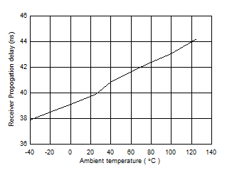
ISO1450 ISO1452 ISO1410 ISO1412 ISO1430 ISO1432 ISO145x Receiver Propagation Delay (ns) Vs. Temperature (C)
VCC1 = 3.3 VVCC2 = 5 V
Figure 7-26 ISO145x Receiver Propagation Delay (ns) Vs. Temperature (C)
ISO1450 ISO1452 ISO1410 ISO1412 ISO1430 ISO1432 ISO145x Receiver VID vs Signaling Rate
For PWD ≤±5%
Figure 7-28 ISO145x Receiver VID vs Signaling Rate
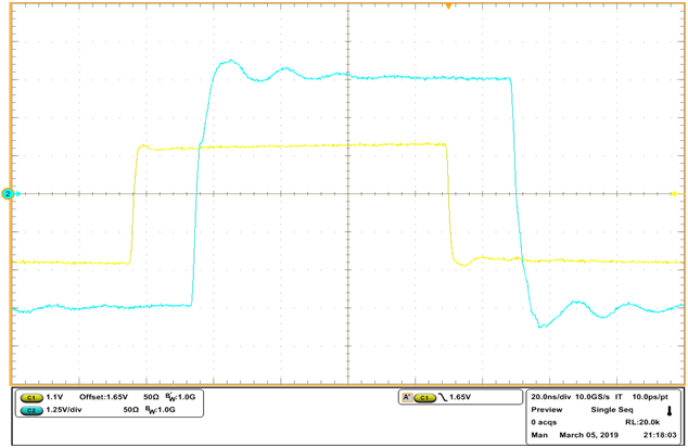
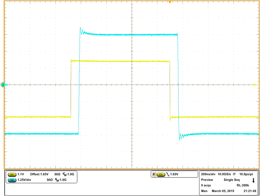
ISO1450 ISO1452 ISO1410 ISO1412 ISO1430 ISO1432 ISO143x Driver Propagation Delay
VCC1 = 3.3 V VCC2 = 5 V TA = 25° C
DE = VCC1
Figure 7-30 ISO143x Driver Propagation Delay
ISO1450 ISO1452 ISO1410 ISO1412 ISO1430 ISO1432 ISO141x Receiver Propagation Delay
VCC1 = 3.3 V VCC2 = 5 V TA = 25° C
DE = GND1 RE = GND1
Figure 7-32 ISO141x Receiver Propagation Delay
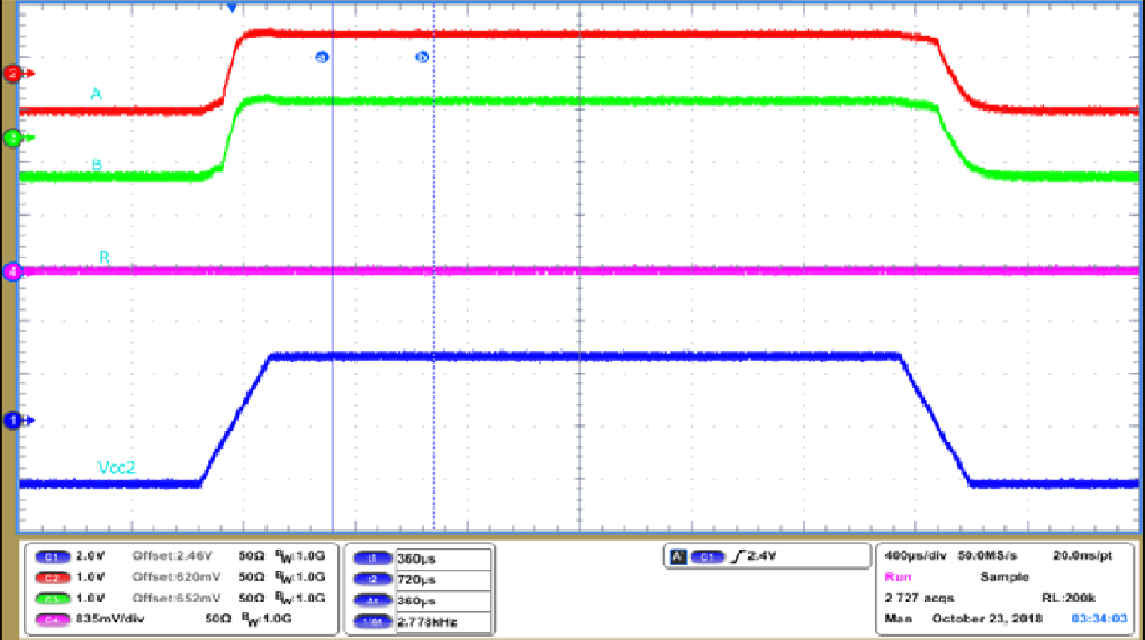
ISO1450 ISO1452 ISO1410 ISO1412 ISO1430 ISO1432 VCC2 Power Up/Power Down - Glitch Free Behavior
Figure 7-34 VCC2 Power Up/Power Down - Glitch Free Behavior