SLLSFG4F December 2019 – June 2024 ISO6740-Q1 , ISO6741-Q1 , ISO6742-Q1
PRODUCTION DATA
- 1
- 1 Features
- 2 Applications
- 3 Description
- 4 Pin Configuration and Functions
-
5 Specifications
- 5.1 Absolute Maximum Ratings
- 5.2 ESD Ratings
- 5.3 Recommended Operating Conditions
- 5.4 Thermal Information
- 5.5 Power Ratings
- 5.6 Insulation Specifications
- 5.7 Safety-Related Certifications
- 5.8 Safety Limiting Values
- 5.9 Electrical Characteristics—5-V Supply
- 5.10 Supply Current Characteristics—5-V Supply
- 5.11 Electrical Characteristics—3.3-V Supply
- 5.12 Supply Current Characteristics—3.3-V Supply
- 5.13 Electrical Characteristics—2.5-V Supply
- 5.14 Supply Current Characteristics—2.5-V Supply
- 5.15 Electrical Characteristics—1.8-V Supply
- 5.16 Supply Current Characteristics—1.8-V Supply
- 5.17 Switching Characteristics—5-V Supply
- 5.18 Switching Characteristics—3.3-V Supply
- 5.19 Switching Characteristics—2.5-V Supply
- 5.20 Switching Characteristics—1.8-V Supply
- 5.21 Insulation Characteristics Curves
- 5.22 Typical Characteristics
- 6 Parameter Measurement Information
- 7 Detailed Description
- 8 Application and Implementation
- 9 Device and Documentation Support
- 10Revision History
- 11Mechanical, Packaging, and Orderable Information
3 Description
The ISO674x-Q1 devices are high-performance, quad-channel digital isolators designed for cost-sensitive applications requiring up to 5000VRMS isolation ratings per UL 1577. These devices are also certified by VDE, TUV, CSA, and CQC.
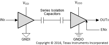
The ISO674x-Q1 devices provide high electromagnetic immunity and low emissions at low power consumption, while isolating CMOS or LVCMOS digital I/Os. Each isolation channel has a logic input and output buffer separated by TI's double capacitive silicon dioxide (SiO2) insulation barrier. These devices come with enable pins which can be used to put the respective outputs in high impedance for multi-controller driving applications. The ISO6740-Q1 device has all four channels in the same direction, the ISO6741-Q1 device has three forward and one reverse-direction channels, and the ISO6742-Q1 device has two forward and two reverse-direction channels. In the event of input power or signal loss, the default output is high for devices without suffix F and low for devices with suffix F. See also Device Functional Modes section.
Used in conjunction with isolated power supplies, the ISO674x-Q1 devices help prevent noise currents on data buses, such as CAN and LIN from damaging sensitive circuitry. Through remarkable chip design and layout techniques, the electromagnetic compatibility of the ISO674x-Q1 devices has been significantly enhanced to ease system-level ESD, EFT, surge, and emissions compliance. The ISO674x-Q1 family of devices is available in a 16-pin SOIC wide-body (DW) package and is a pin-to-pin upgrade to the older generations.
| PART NUMBER | PACKAGE(1) | BODY SIZE (NOM) | PACKAGE SIZE(2) |
|---|---|---|---|
| ISO6740-Q1,
ISO6740F-Q1 ISO6741-Q1, ISO6741F-Q1 ISO6742-Q1, ISO6742F-Q1 |
DW (SOIC, 16) | 10.30mm × 7.50mm | 10.30mm × 10.30mm |
| ISO6742-Q1, ISO6742F-Q1 | DWW (Extra wide SOIC, 16)(3) | 10.30mm × 14.0mm | 10.30mm × 17.25mm |

| VCCI=Input supply, VCCO=Output
supply GNDI=Input ground, GNDO=Output ground |