SLLSFJ1D February 2022 – March 2023 TIOL112 , TIOL1123 , TIOL1125
PRODUCTION DATA
- 1 Features
- 2 Applications
- 3 Description
- 4 Revision History
- 5 Pin Configuration and Functions
- 6 Specifications
- 7 Parameter Measurement Information
-
8 Detailed Description
- 8.1 Overview
- 8.2 Functional Block Diagrams
- 8.3
Feature Description
- 8.3.1 Wake-Up Detection
- 8.3.2 Current Limit Configuration
- 8.3.3 Current Fault Detection, Indication and Auto Recovery
- 8.3.4 Thermal Warning, Thermal Shutdown
- 8.3.5 Fault Reporting (NFAULT)
- 8.3.6 Transceiver Function Tables
- 8.3.7 The Integrated Voltage Regulator (LDO)
- 8.3.8 Reverse Polarity Protection
- 8.3.9 Integrated Surge Protection and Transient Waveform Tolerance
- 8.3.10 Power Up Sequence (TIOL112)
- 8.3.11 Undervoltage Lock-Out (UVLO)
- 8.4 Device Functional Modes
- 9 Application and Implementation
- 10Device and Documentation Support
- 11Mechanical, Packaging, and Orderable Information
7 Parameter Measurement Information
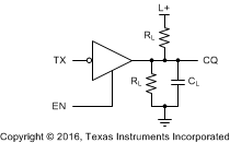
 Figure 7-1 Test
Circuit for Driver Switching
 Figure 7-2 Waveforms
for Driver Output Switching Measurements
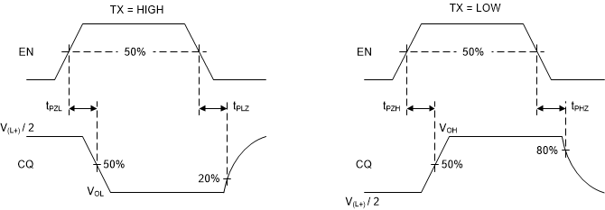
 Figure 7-3 Waveforms
for Driver Enable or Disable Time Measurements
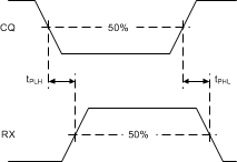
 Figure 7-4 Receiver
Switching Measurements
Figure 7-5 Overcurrent and Wake Conditions for EN = H and ILIM_ADJ = 10 kΩ to 110 kΩ,
TX = H (Full Lines); and TX = L (Red Dotted Lines)
TX = H (Full Lines); and TX = L (Red Dotted Lines)
Figure 7-6 Wake Conditions for EN = L, RX = H (Full
Lines); and RX = L (Red Dotted Lines)
Figure 7-7 Overcurrent and Wake Conditions for EN = H and ILIM_ADJ is floating, TX = H (Full Lines); and TX = L (Red Dotted Lines)