SLLSFL4B february   2022  – june 2023 TIOS102 , TIOS1023 , TIOS1025

PRODUCTION DATA  

  1.   1
  2. Features
  3. Applications
  4. Description
  5. Revision History
  6. Pin Configuration and Functions
  7. Specifications
    1. 6.1 Absolute Maximum Ratings
    2. 6.2 ESD Ratings
    3. 6.3 ESD Ratings - IEC Specifications
    4. 6.4 Recommended Operating Conditions
    5. 6.5 Thermal Information
    6. 6.6 Electrical Characteristics
    7. 6.7 Switching Characteristics
    8. 6.8 Typical Characteristics
  8. Parameter Measurement Information
  9. Detailed Description
    1. 8.1 Overview
    2. 8.2 Functional Block Diagrams
    3. 8.3 Feature Description
      1. 8.3.1  Current Limit Configuration
      2. 8.3.2  Current Fault Detection, Indication and Auto Recovery
      3. 8.3.3  Thermal Warning, Thermal Shutdown
      4. 8.3.4  Fault Reporting (NFAULT)
      5. 8.3.5  Device Function Tables
      6. 8.3.6  The Integrated Voltage Regulator (LDO)
      7. 8.3.7  Reverse Polarity Protection
      8. 8.3.8  Integrated Surge Protection and Transient Waveform Tolerance
      9. 8.3.9  Power Up Sequence
      10. 8.3.10 Undervoltage Lock-Out (UVLO)
    4. 8.4 Device Functional Modes
      1. 8.4.1 NPN Configuration (N-Switch Mode)
      2. 8.4.2 PNP Configuration (P-Switch Mode)
      3. 8.4.3 Push-Pull Mode
  10. Application Information Disclaimer
    1. 9.1 Application Information
    2. 9.2 Typical Application
      1. 9.2.1 Design Requirements
      2. 9.2.2 Detailed Design Procedure
        1. 9.2.2.1 Maximum Junction Temperature Check
        2. 9.2.2.2 Driving Capacitive Loads
        3. 9.2.2.3 Driving Inductive Loads
      3. 9.2.3 Application Curves
  11. 10Power Supply Recommendations
  12. 11Layout
    1. 11.1 Layout Guidelines
    2. 11.2 Layout Example
  13. 12Device and Documentation Support
    1. 12.1 Receiving Notification of Documentation Updates
    2. 12.2 Support Resources
    3. 12.3 Trademarks
    4. 12.4 Electrostatic Discharge Caution
    5. 12.5 Glossary
  14. 13Mechanical, Packaging, and Orderable Information
    1. 13.1 Mechanical Data

Application Curves

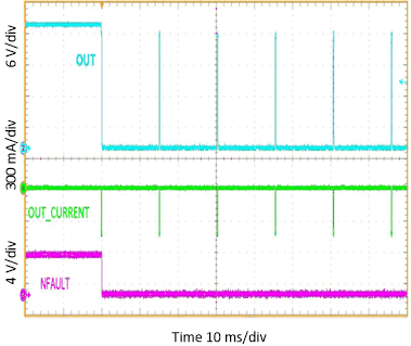
GUID-E58E9604-6444-4167-8311-DFDC03EC5A70-low.gif
Figure 9-4 OUT In Current Fault Auto Recovery, Low Side Mode
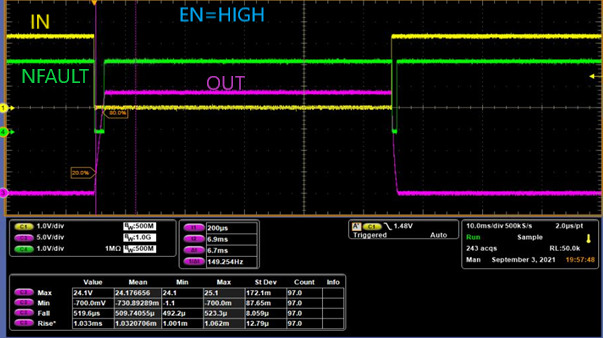
GUID-20221117-SS0I-KJGP-06HJ-NN1DHS5BQGRB-low.png
VCC = 36 V L = 1.5 H RL = 360 Ω
RSET = 10 kΩ TA = 25 °C
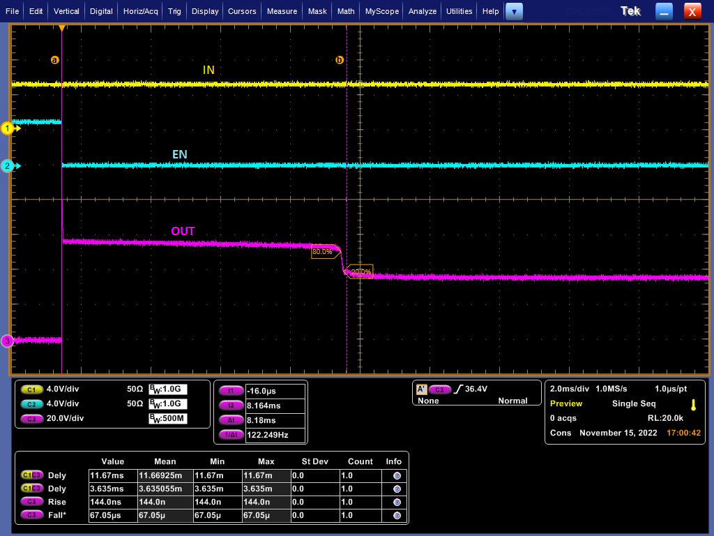
Figure 9-6 OUT Driving Inductive Load, High Side Mode (PNP)
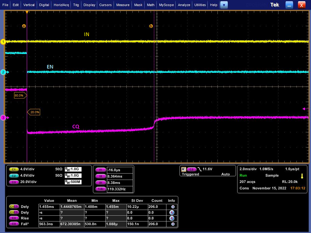
GUID-20221114-SS0I-MRGM-9PDM-5RBDMLFRLW0J-low.png
NFAULT indicated for the duration of charging and discharging of the capacitor but driver is not disabled when ILIM_ADJ is floating.
VCC = 24 V CL = 20 uF RL = 100 Ω RSET = 1 MΩ (ILIM_ADJ Floating) TA = 25 °C
Figure 9-8 OUT Driving Capacitive Load, Push-Pull Mode
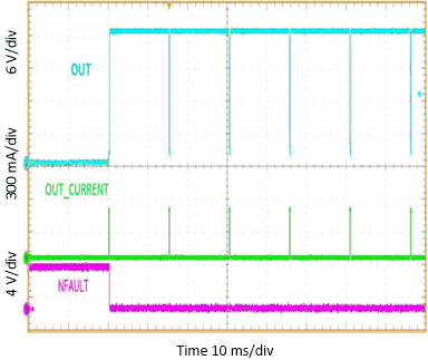
GUID-24193C3C-E04E-4A9D-8E98-CDCE8A0C5DEF-low.gif
Figure 9-5 OUT In Current Fault Auto Recovery, High Side Mode
GUID-20221117-SS0I-9QPM-SWX1-7LGJTHHRSNWB-low.png
VCC = 36 V L = 1.5 H RL = 360 Ω
RSET = 10 kΩ TA = 25 °C
Figure 9-7 OUT Driving Inductive Load, Low Side Mode (NPN)